Visual inspection of optical elements

a technology of optical elements and visual inspection, applied in the field of optical imaging devices, can solve the problems of annoying refocus of technical staff members, and achieve the effect of simplifying the adjustment of focus and performing more quickly

Inactive Publication Date: 2008-03-27
AGILENT TECH INC
View PDF17 Cites 15 Cited by
  • Summary
  • Abstract
  • Description
  • Claims
  • Application Information

AI Technical Summary

Benefits of technology

[0006]The focus evaluation mechanism according to embodiments of the present invention allows to adjust the focus of the acquired image more quickly. An image of good definition is obtained more quickly. An increased number of optical elements can be checked per unit time, and the throughput is increased. Besides that, it is rather annoying for a technical staff member to refocus many times before a respective fault is found. In this respect, the focussing aid provided by embodiments of the present invention is capable of improving the conditions of work.
[0009]According to another preferred embodiment, the optical imaging device is combined with a measuring unit. The measuring unit allows determining an optical property of the optical element or the fiber optic network, whereas the optical imaging device acquires the imaging data for visualizing the surface of the optical element. By combining the two approaches, a quick and accurate examination of the optical elements is possible. A device that combines the imaging functionality with a measuring capability permits to reduce the space required for the measurement set-up. One screen is used for displaying both images and measurement results.
[0013]In a preferred embodiment, instead of utilizing the entire image data for deriving the focus evaluation value, only a small part of the image data in a predefined region of interest (ROI) is used for evaluating the image definition. As a consequence, the computational burden is reduced.
[0021]The focus evaluation value that has been determined in accordance with one of the possibilities that have been described above can be used as a focussing aid for either automatically or manually adjusting the focus. Preferably, in case the focus is adjusted manually, a feedback signal indicating the instantaneous image definition is communicated to the user. For this purpose, the optical imaging device might comprise a feedback unit adapted for generating a feedback signal that corresponds to the focus evaluation value. In accordance with the feedback signal, the user can adjust the focus until an optimum image definition is reached. Hence, the adjustment of the focus is simplified and can be performed more quickly.
[0022]According to a preferred embodiment, the optical imaging device comprises an acoustic or tactile feedback unit that provides an acoustic or tactile feedback signal to the user. In order to find the optimum image definition, the user can vary the focus while listening to the acoustic or sensing the tactile feedback signal. In this embodiment, the user does not have to watch a display while manually adjusting the focus.
[0024]Alternatively, the focus of the imaging unit can be adjusted automatically. In a preferred embodiment, the optical imaging device comprises an autofocus control module that is adapted for varying the focus until an optimum image definition is accomplished. Focussing is carried out automatically, and the user does not have to care about adjusting the focus.

Problems solved by technology

Besides that, it is rather annoying for a technical staff member to refocus many times before a respective fault is found.

Method used


Image

  • Visual inspection of optical elements
  • Visual inspection of optical elements
  • Visual inspection of optical elements

Examples


Embodiment Construction

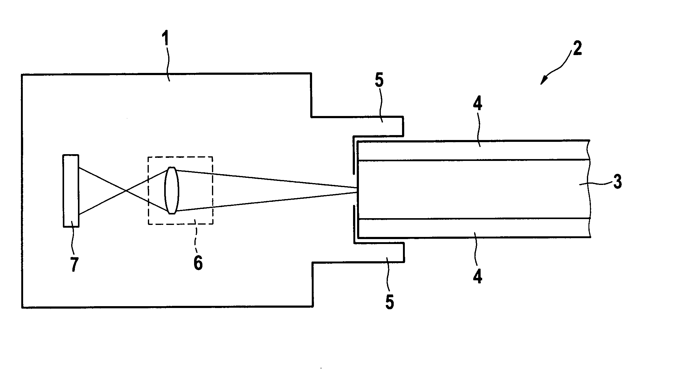
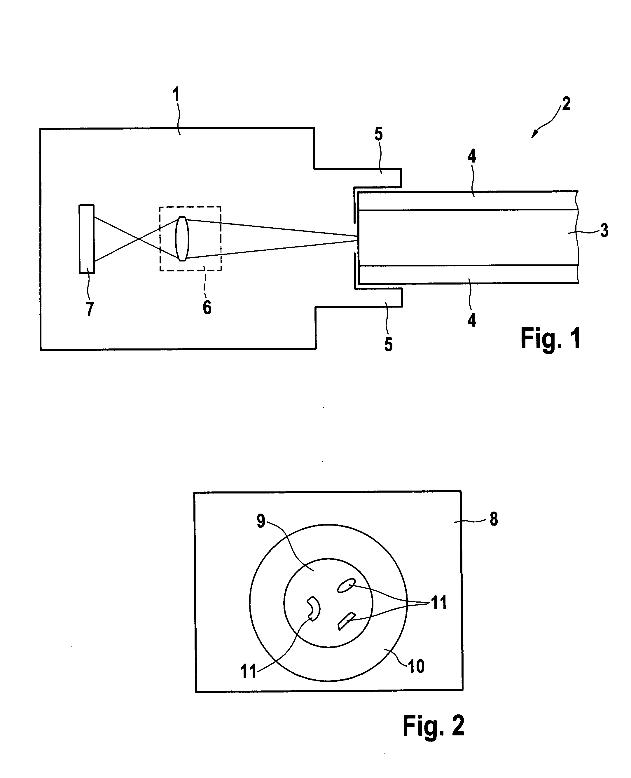
[0040]FIG. 1 shows an optical imaging unit 1 that allows to visually inspect an optical element 2. The optical imaging unit 1 is employed for visually inspecting the surface of an optical fiber 3 that is surrounded by a metal or ceramic ferule 4. For this purpose, the optical imaging device 1 comprises a connector interface 5. The optical imaging unit 1 might e.g. be implemented as an electronic video microscope comprising an objective lens system 6 and an imaging unit 7, which might e.g. comprise a light sensitive chip that converts an optical image into corresponding imaging signals. Optionally, the imaging signals can be subjected to some kind of image processing. Then, the acquired image is displayed on a monitor. Typically, in field applications, an electronic video microscope consisting of camera unit, monitor, and battery pack is utilized for checking optical fiber connections.

[0041]FIG. 2 shows an image 8 of an optical element that has been acquired by the optical imaging un...


PUM

PropertyMeasurementUnit
optical propertyaaaaaaaaaa
optical time domain reflectometeraaaaaaaaaa
dispersion measurementsaaaaaaaaaa

Abstract

An optical imaging device for visually inspecting an optical element is described. The optical imaging device comprises an optical connector interface adapted for connecting the optical imaging device to the optical element, an imaging unit adapted for acquiring image data of the optical element's surface, and a display for visualizing the image data. The optical imaging device further comprises a focus evaluation facility adapted for deriving a focus evaluation value indicating the instantaneous image definition of the acquired image, said focus evaluation value being derived from at least one of: the acquired image data itself and additional signals related to the position of the imaging unit relative to the surface of the optical element. The focus evaluation value is usable as a focussing aid for either automatically or manually adjusting the focus.

Description

BACKGROUND OF THE INVENTION[0001]The present invention relates to an optical imaging device for visually inspecting an optical element, and to a method for visually inspecting an optical element. Furthermore, the present invention relates to a software program or product adapted for being executed on a processing unit of an optical imaging device.[0002]Optical elements are generally very susceptible for contamination, dirt, scratches, and so on, which can cause faults such a increased bit error rate, signal degradation, or increased insertion loss. A visual inspection of optical elements might therefore be applied. Typically, such visual inspection is carried out using an optical imaging device adapted for field applications.SUMMARY OF THE INVENTION[0003]It is an object of the invention to improve the visual inspection of optical elements. The object is solved by the independent claims. Preferred embodiments are shown by the dependent claims.[0004]An optical imaging device according...

Claims


Application Information

Patent Timeline
Patent Type & Authority Applications(United States)
IPC IPC(8): G01N21/00G02B27/40
CPCG02B7/36G01M11/3154
Inventor JAHN, ROBERTBELLER, JOSEFHOFFMANN, PETER
Owner AGILENT TECH INC
Why Eureka
Try Eureka