Charged particle beam scanning method and charged particle beam apparatus

a technology of charged particle beam and scanning method, which is applied in the direction of material analysis using wave/particle radiation, instruments, nuclear engineering, etc., can solve the problems of not being able to move the scan position the degree of image shift error differs point by point, and the scan position cannot sometimes be moved to a desired location

Active Publication Date: 2008-03-27
HITACHI HIGH-TECH CORP
View PDF3 Cites 18 Cited by
  • Summary
  • Abstract
  • Description
  • Claims
  • Application Information

AI Technical Summary

Benefits of technology

[0006] In connection with a charged particle beam scanning method for deflecting the scan position of a charged particle beam and a charged particle beam apparatus, it is an object of the present invention to provide charged particle beam scanning method and charged particle beam apparatus which can settle the scan position at a proper location within a deflectable range of charged particle beam scan position.
[0007] Further, the present invention provides method and apparatus which can set a proper optical condition of a charged particle beam within the deflectable range of charged particle beam scan position.
[0010] Through the above example of the present invention, accurate deflection of the scan position can be achieved within the deflectable region of the charged particle beam scan position.

Problems solved by technology

The image shift, however, is a technique of deviating an electron beam from the electron beam optical axis (meaning, in the present specification, an electron beam trajectory through which the electron beam can reach a specimen without being deflected) and therefore, raises a problem that under the influence of, for example, deflective function of lens, the scan position cannot sometimes be moved to a desired location.
In the technique of precisely measuring in advance the sensitivity to image shift and correcting the image shift amount as explained in US2006 / 0219907AI, there arises a problem that an instance cannot be dealt with in which a plurality of measuring points exist in the deflection region of image shift and the degree of image shift error differs point by point.

Method used


Image

  • Charged particle beam scanning method and charged particle beam apparatus
  • Charged particle beam scanning method and charged particle beam apparatus
  • Charged particle beam scanning method and charged particle beam apparatus

Examples


embodiment 2

[0062] By setting the measuring range of error amount to a range wider than that of movement amounts of charged particle beam allowed for the apparatus, correction can be made highly accurately although depending on a correction calculation method. For example, when a range wider than the X movement amount range and Y movement amount range on the apparatus is taken as shown at region 47 in FIG. 11, the accuracy of calculation of correction for error amount can be ameliorated. For example, a method for correction calculation is employed according to which four location points are extracted out of points indicated in FIG. 10 to prepare a quadrilateral and an equation representative of the quadrilateral is used to calculate an error amount at a position inside it. If, in this case, correction is desired to be made at all areas as shown in FIG. 11, information regarding a region outside the movement range is needed. And in this case an error amount is calculated on the basis of address ...

embodiment 3

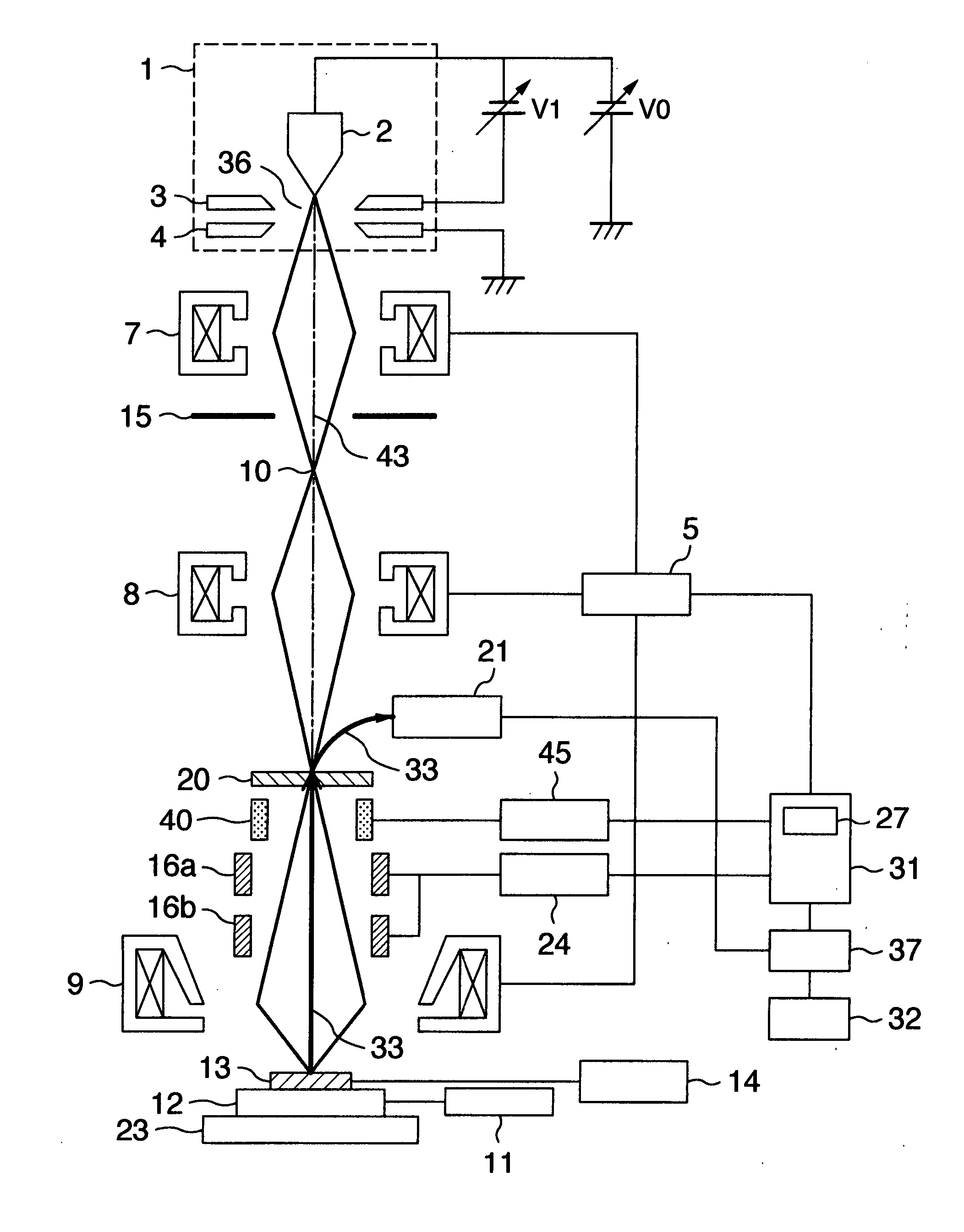
[0077] A semiconductor wafer as representing the specimen 13 is not always flush, having different heights. Therefore, the movement amount of scan position of electron beam 36 needs to be controlled cooperatively with the height. For example, when the deflector 41 is used for control of the scan position, the movement amount will change with different specimen heights even if the same current or voltage is applied to the deflector 41.

[0078] Further, if the distance over which movement is made is large in moving the scan position of electron beam 36, an aberration due to curvature of field results in an astigmatism and the like and a change develops. This impairs clarity of image, that is, an image blurs, degrading the accuracy of measurement of the centroid of the target object. Then, depending on the movement distance of electron beam 36, an aberration such as aberration due to curvature of field or astigmatism responsible for image blur needs to be adjusted.

[0079] If, in the cou...

embodiment 4

[0088] Recently, of semiconductor wafers, a wafer of the type in which electrification is accumulated in a stationary fashion on the overall wafer surface can be seen here and there. The electrification is known as being difficult to be removed by grounding. Causes of this stationary electrification is accounted for by the fact that, for example, a polar substance inside resist is polarized by friction during resist coating by means of a spin coater and stationary potential results or that the electrification is based on an etching process using plasma.

[0089] The electrification accumulated in a stationary fashion over a wide wafer area (sometimes termed global electrification hereinafter) tends to exhibit potential which is the highest in the center of the wafer and decreases toward the edge of the wafer. Potential remaining on the specimen surface forms a lens based on the principle of formation of electrostatic lens. Since the potential of the global electrification differs for ...


PUM


Abstract

In a method of scanning a charged particle beam which can position the scan position to a proper location inside a deflectable range of the scan position of charged particle beam, the scan position of charged particle beam is deflected to a plurality of target objects inside a scan position deflectable region and on the basis of a shift of a target object at a scan location after deflection, the deflection amount at the scan location is corrected.

Description

BACKGROUND OF THE INVENTION [0001] The present invention relates to a method of scanning a charged particle beam and to a charged particle beam apparatus and more particularly, to method and apparatus for moving the scan position of a charged particle beam by means of a deflector. [0002] A technique for moving the scan position of an electron beam on a specimen by the deflector (sometimes termed image shift) has been known. As the technique is compared with a technique for moving the scan position of an electron beam on a specimen by means of a specimen stage, the technique using the deflector has features that it can move the electron beam scan position highly precisely and speedily. As regards the image shift as above, US 2006 / 0219907A1 explains a technique of precisely measuring in advance an amount of movement of an electron beam on a specimen (an image shift amount) in response to a control parameter (control current) of an image shift deflector, that is, measuring a sensitivit...

Claims


Application Information

Patent Timeline
Patent Type & Authority Applications(United States)
IPC IPC(8): G21K5/04
CPCH01J37/265H01J37/28H01J2237/3045H01J2237/2826H01J2237/15
Inventor SASAKI, YUKOEZUMI, MAKOTONISHIHARA, MAKOTOKAWAI, TSUTOMUYANOKURA, TOSHIAKI
Owner HITACHI HIGH-TECH CORP
Why Eureka
Try Eureka