
Nanostructure and manufacturing method for same

a manufacturing method and nanotechnology, applied in the field of nanostructure, can solve the problems of high manufacturing cost, inability to provide high yield, and manufacturing methods in prior arts based on two-dimensional processes, and achieve the effect of low cos

Inactive Publication Date: 2008-03-27
THE FUJIKURA CABLE WORKS LTD +1
View PDF3 Cites 0 Cited by
  • Summary
  • Abstract
  • Description
  • Claims
  • Application Information

AI Technical Summary

Benefits of technology

[0030] The manufacturing method of the invention may be used to mass produce three-dimensional nanostructures which does not have a closest packing structure at a low cost.

Problems solved by technology

However, those prior arts require high manufacturing cost and cannot provide a high yield.
In addition, manufacturing methods in the prior arts are based on a two-dimensional process and cannot be appropriately used in the mass production of three-dimensionally structured materials.
However, a general process of self organization using isotropic particles only achieves a closest packing structure of fine particles.

Method used


Image

  • Nanostructure and manufacturing method for same
  • Nanostructure and manufacturing method for same
  • Nanostructure and manufacturing method for same

Examples


example 1

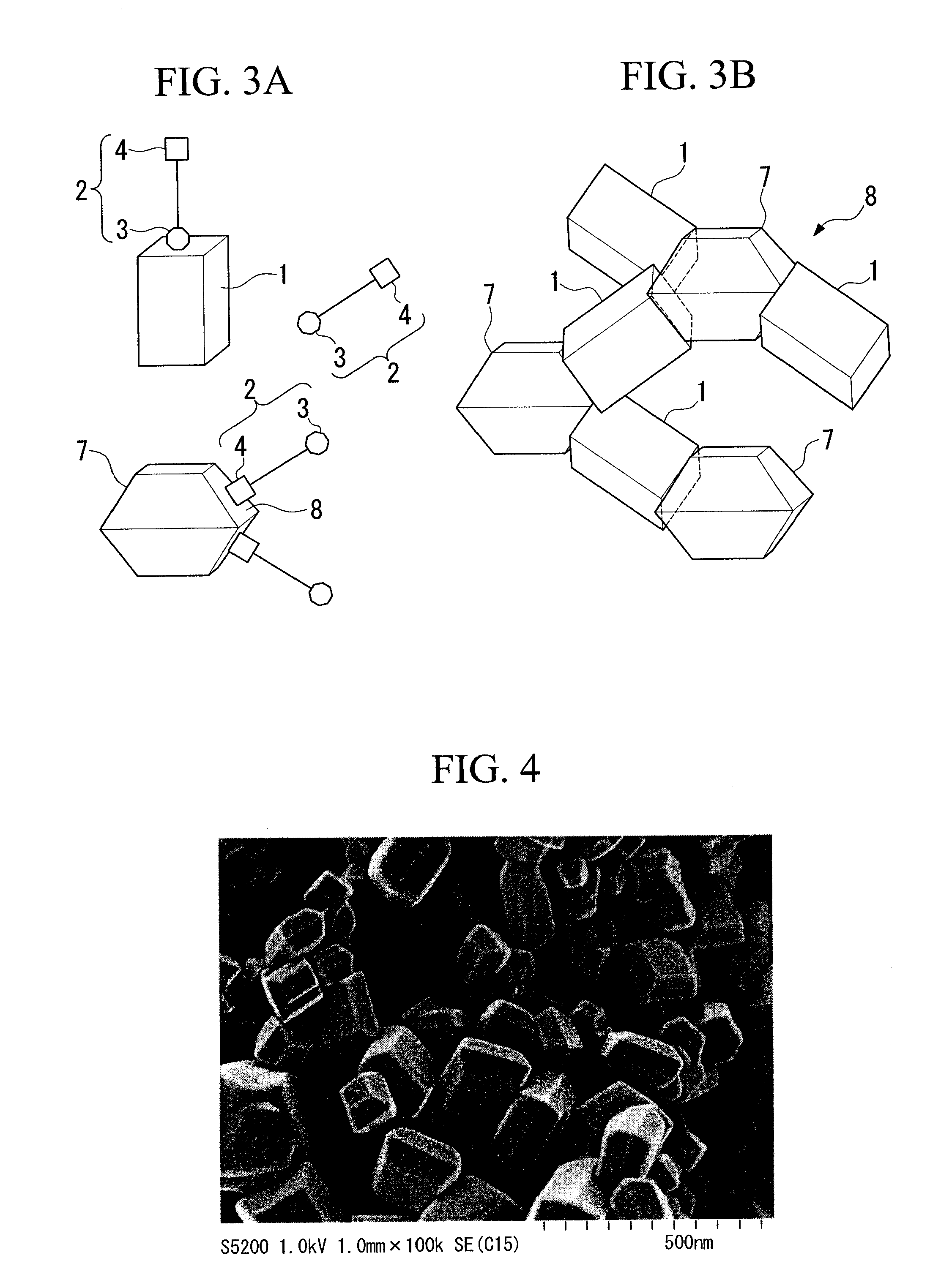
[0070] Decahedral titanium oxide particles shown in FIG. 4 were synthesized by a CVD method using titanium tetrachloride as a raw material. Titanium oxide belongs to an tetragonal system, and the crystal surface forming a decahedron comprises square faces equivalent to the (001) plane and trapezoidal faces equivalent to the (101) plane. In the following description, the term (101) planes represents crystal faces equivalent to the (101) plane. Average particle size of the decahedral titanium oxide was 100 nm.

[0071] Next, the decahedral titanium oxide particles were dispersed in a 2-propanol solution containing gold chloride acid. After photo radiation of the solution using a high pressure mercury vapor lamp, about 20% of gold was photo-deposited on the surface of the decahedral titanium oxide particles. A few drops of solution were dried on a slide glass, and were subsequently observed by a Scanning Electron Microscope as shown in FIG. 5.

[0072] The result of SEM observation shows t...

example 2

[0073] Silica particles having spherical shapes of approximately 500 nm in seize were prepared from a commercial product. The surface of the silica particles were modified with silane coupling agents (3-mercaptopropyltrimethoxysilane). After the modification, the methoxy groups of the silane coupling agents were connected to the silica surfaces, and the silica particles had mercapto groups on their surfaces.

[0074] Next, the silica particles were added to the solution in which gold-bearing decahedral titanium oxide particles prepared in the Example 1 were dispersed. Nanostructures were formed after agitating the solution. A schematic drawing and SEM image of the nanostructure obtained after the agitation are shown in FIGS. 6A and B.

[0075] The result of SEM observation confirmed that spherical silica particles are connected to the (101) planes of the decahedral titanium oxide particles. Thus the formation of the nanostructure can be explained by the selective bonding of mercapto gro...


PUM

PropertyMeasurementUnit
sizeaaaaaaaaaa
sizeaaaaaaaaaa
particle sizeaaaaaaaaaa

Abstract

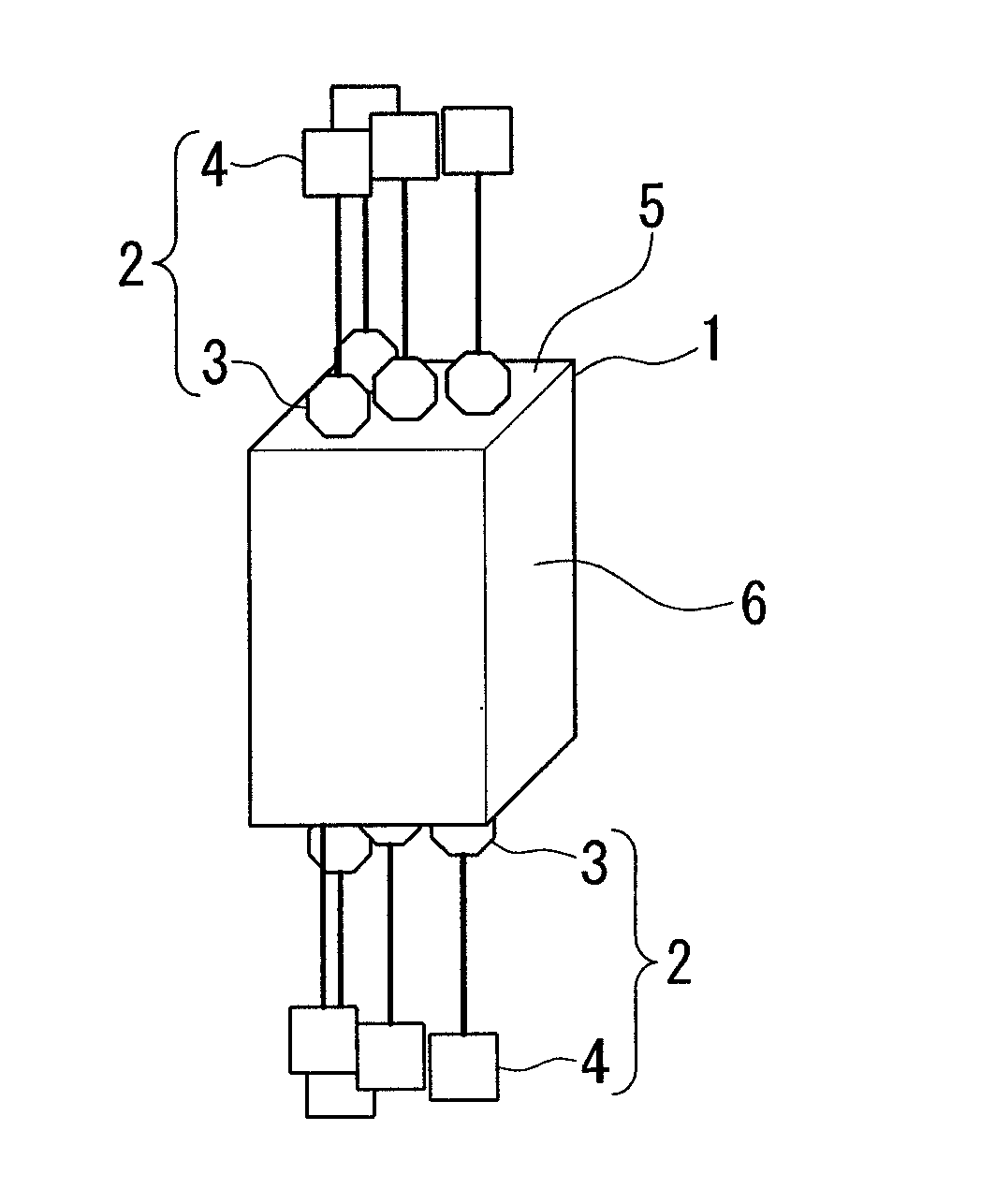
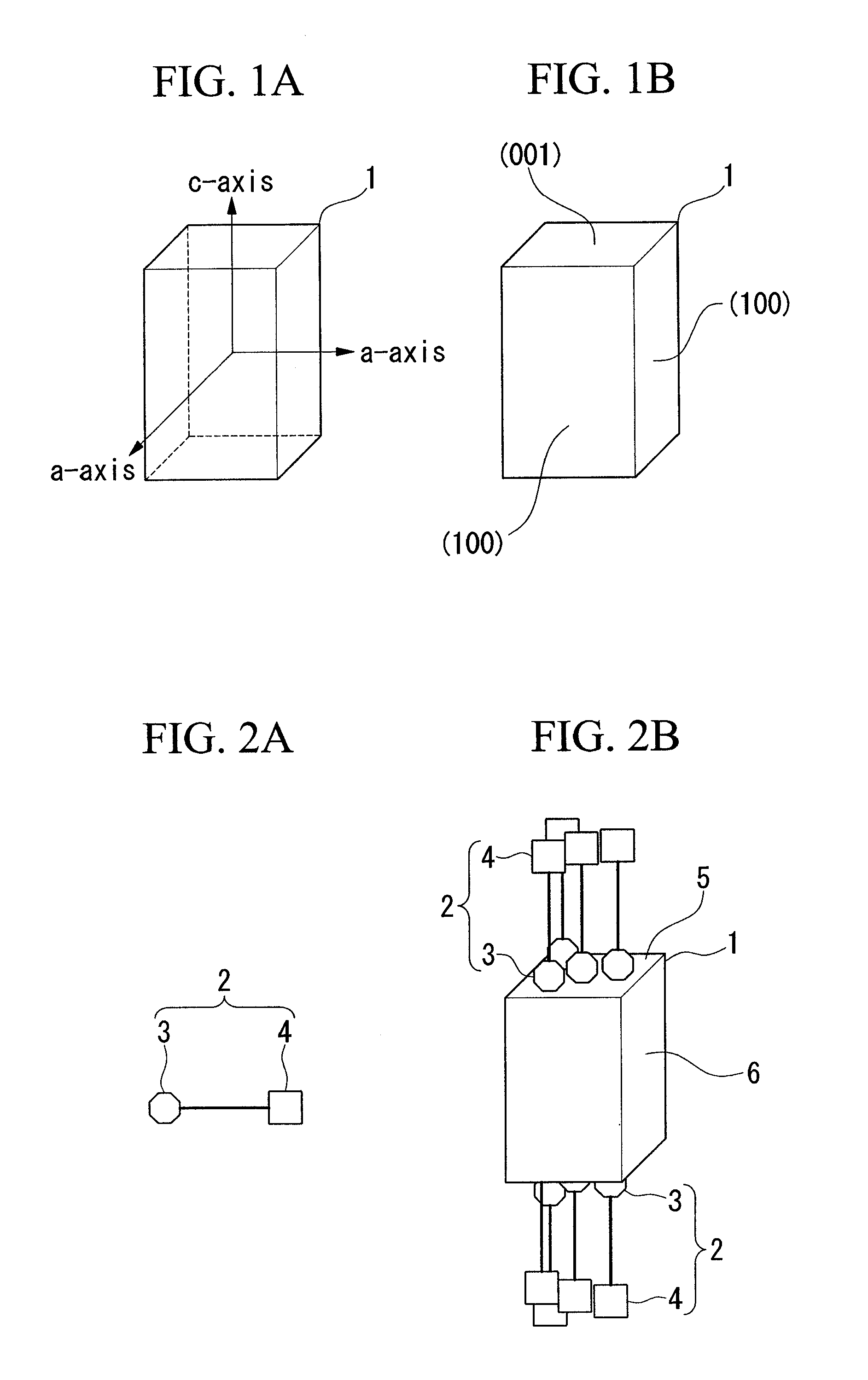
The invention relates to nanostructure and its manufacturing method. In the manufacturing method of a nanostructure, first anisotropic crystalline particles, connectors having end to be connected to a specific crystal face of each of said crystalline particles, and second particles to be connected to the other end of each of said connectors are prepared. First ends of the connectors are connected to specific crystal faces of the first crystalline particles, and simultaneously or before or after the connection, the second ends of the connectors are connected to the second particles. A nanostructure formed by this method has a three-dimensional structure which does not have a closest packing structure.

Description

BACKGROUND OF THE INVENTION [0001] 1. Field of the Invention [0002] The invention relates to a nanostructure as an advanced functional material having a nano sized structure, and a manufacturing method of the nanostructure. [0003] Priority is claimed on Japanese Patent Application No. 2004-343117, filed Nov. 26, 2004, the content of which is incorporated herein by reference. [0004] 2. Description of the Related Art [0005] As is widely known, under a size smaller than a specific value, thin films, thin wires, pores, and dots of a metal or a semiconductor exhibit, specific electronic, optical, and chemical properties. Based on that knowledge, a nanostructure of several ten to hundred nanometers in size is expected as an advanced functional material, and extensive study has been carried out on such a nanostructure (ex. Japanese Unexamined Patent Application, First Publication No. 2003-332561, Japanese Unexamined Patent Application, First Publication No. 2003-266400). [0006] Japanese Un...

Claims


Application Information

Patent Timeline
Patent Type & Authority Applications(United States)
IPC IPC(8): C23C14/28
CPCC23C18/14C23C18/143
Inventor TERADA, YOSHIHIROKAMIKATANO, MITSURUHIMENO, KUNIHARUOHTANI, BUNSHOYAMAGAMI, TAKAMUNETORIMOTO, TSUKASA
Owner THE FUJIKURA CABLE WORKS LTD
Learn More