Processing termination detection method and apparatus

a detection method and technology of processing termination, applied in the field of processing termination detection methods and apparatuses, can solve the problems of low throughput, difficult to carry out a proper changeover from the first etching step to the low etching rate condition in proper timing, and difficult to achieve accurate changeover of etching ra

Inactive Publication Date: 2008-04-03
TOKYO ELECTRON LTD
View PDF9 Cites 24 Cited by
  • Summary
  • Abstract
  • Description
  • Claims
  • Application Information

AI Technical Summary

Benefits of technology

[0013]The present invention provides processing termination detection method and apparatus capable of accurately performi

Problems solved by technology

In order to prevent undesired formation of the notch N, the single crystal silicon layer P must be etched with a low etch rate to suppress the side surface of the through-hole H from being etched after exposure of the silicon oxide layer O. However, such etching condition results in low throughput.
However, the estimation of this method cannot accurately determine that the single cryst

Method used


Image

  • Processing termination detection method and apparatus
  • Processing termination detection method and apparatus
  • Processing termination detection method and apparatus

Examples


Embodiment Construction

[0046]The present invention will now be described in detail below with reference to the drawings showing a preferred embodiment thereof.

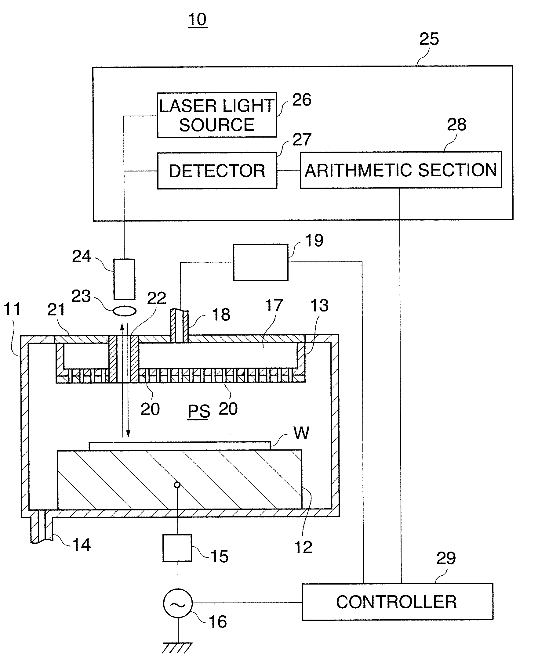
[0047]First, an explanation will be given of a substrate processing apparatus to which a processing termination detection method of this embodiment is applied. This substrate processing apparatus is designed to perform plasma etching on a semiconductor wafer W as a substrate (hereinafter simply referred to as the “wafer W”).

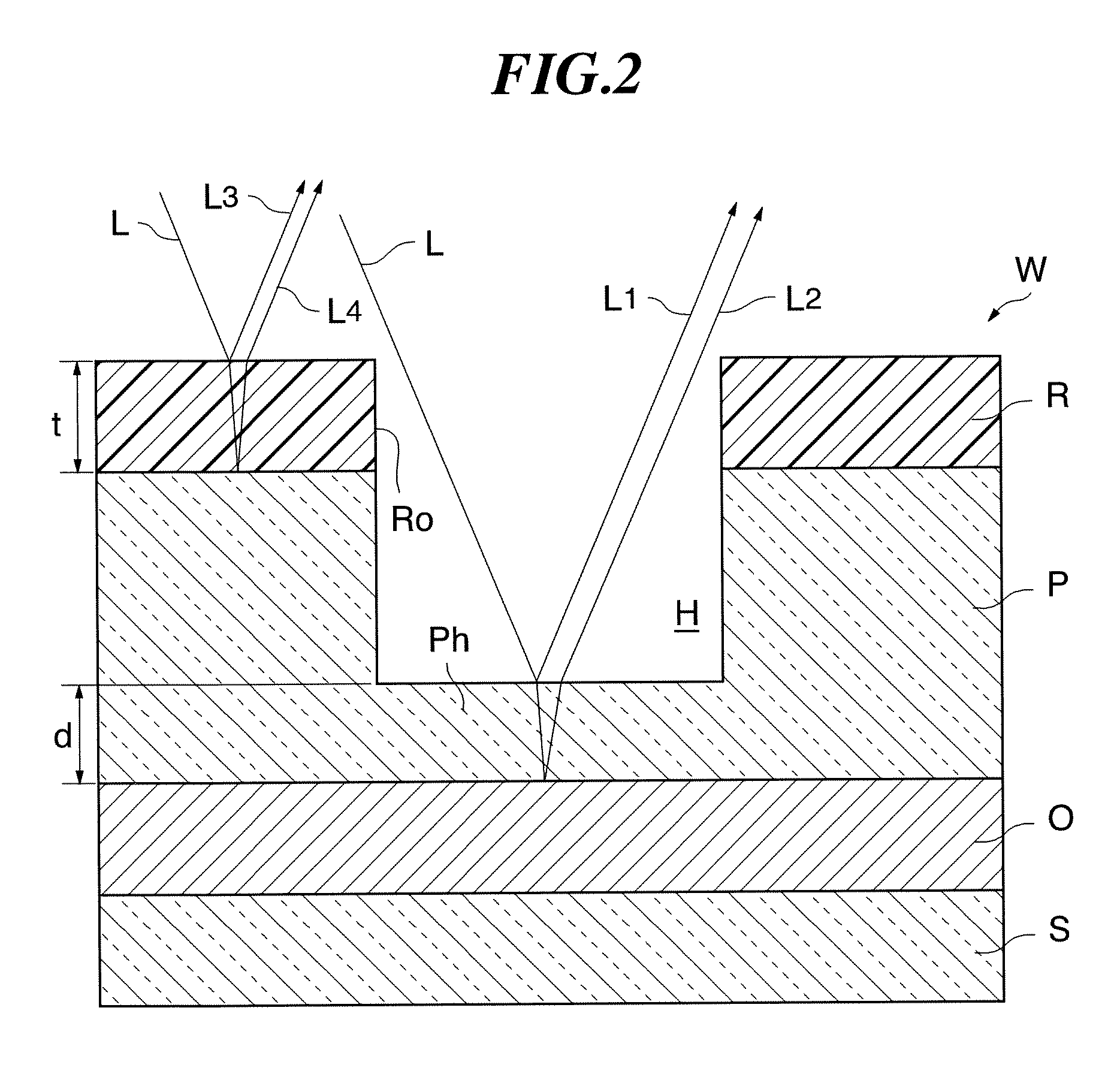
[0048]As shown in FIG. 2, which will be explained in detail later, the wafer W includes, as an insulation layer, a silicon oxide layer O (underlayer) between a single crystal silicon layer S and a single crystal silicon layer P (a to-be-processed layer) and includes a resist layer R (mask layer) formed on the silicon layer P and formed with an opening portion Ro in a predetermined pattern.

[0049]FIG. 1 is a section view schematically showing the construction of a substrate processing apparatus to which is applied a processing term...


PUM


Abstract

A processing termination detection method capable of accurately performing changeover of etch rates when a residual film thickness of a to-be-processed layer decreases to a predetermined value. A substrate processing apparatus starts first etching to form a through-hole in a single crystal silicon layer of a wafer. A processing termination detection apparatus irradiates laser light comprised of red to near-infrared light onto the wafer and performs a frequency analysis of reflected light received from the wafer. When the intensity, represented in a result of the frequency analysis, in a frequency band corresponding to residual layer interference light has exceeded a threshold value, second etching is started to remove a through hole formation portion of the single crystal silicon layer to cause a silicon oxide layer to be exposed.

Description

BACKGROUND OF THE INVENTION[0001]1. Field of the Invention[0002]The present invention relates to processing termination detection method and apparatus, and more particularly, to processing termination detection method and apparatus for detecting a termination point of etching on a substrate.[0003]2. Description of the Related Art[0004]Three-dimensional mounting is recently becoming a mainstream of semiconductor device packaging technology, in which a plurality of chips are mounted in layers. In the three-dimensional mounting, an SOI (silicon-on-insulator) substrate is frequently used, which is comprised of a single crystal silicon layer S, a silicon oxide layer O, and a single crystal silicon layer P, as shown in FIG. 10, and in which a resist layer R is formed in a predetermined pattern on the silicon layer P.[0005]For the three-dimensional mounting, a through-hole H is formed by etching in the SOI substrate, and Cu or the like is filled into the through-hole H for chip connection....

Claims


Application Information

Patent Timeline
IPC IPC(8): H01L21/66H01L21/67
CPCH01L22/26H01L21/67253
Inventor SAITO, SUSUMU
Owner TOKYO ELECTRON LTD
Why Eureka
Try Eureka