Semiconductor device

a semiconductor chip and device technology, applied in the manufacture of printed circuits, printed circuit aspects, basic electric elements, etc., can solve the problems of inability to control the cutting suspension, inability to control the cutting, and the manufacture cost of the semiconductor chip is inevitably increased, so as to reduce the manufacturing cost and the freedom degree of the bottom wiring of the semiconductor chip. , the effect of low cos

Inactive Publication Date: 2008-04-03
LAPIS SEMICON CO LTD
View PDF0 Cites 4 Cited by
  • Summary
  • Abstract
  • Description
  • Claims
  • Application Information

AI Technical Summary

Benefits of technology

[0007]The present invention has been made in consideration of the above circumstances, and accordingly, the object of the present invention is to provide a structure of a semiconductor device that contributes to reduction of the manufacture cost thereof.
[0008]Moreover, another object of the present invention is to provide a method of manufacturing a semiconductor device that contributes to reduction of the manufacture cost thereof.
[0020]In the present invention, since cutout processing can be stopped in the middle of the extending conductive portions, there is no need to perform the position control of cutting precisely in comparison with the prior art. That is, the margin in the depth direction at the moment of cutting the cutout portion can be secured. As a result, a relatively low-cost (not so highly precise) machine can be used, and it becomes possible to aim at the reduction of the manufacture cost.
[0021]Moreover, there is also an advantage that the freedom degree of bottom wiring of a semiconductor chip is improved, by choosing the position of the extending conductive portions to be arranged on the bottom of the semiconductor chip.

Problems solved by technology

However, when a cutout is formed by use of the router for cutout processing (inner layer cutting), it has been difficult to control to suspend cutting at the moment when the bit of the router reaches the surface of the inner layer, and a highly precise machine was required for it.
For this reason, its manufacture cost has inevitably increased.

Method used


Image

  • Semiconductor device
  • Semiconductor device
  • Semiconductor device

Examples


Embodiment Construction

[0040]In the following detailed description of the preferred embodiments, reference is made to the accompanying drawings which form a part hereof, and in which is shown by way of illustration specific preferred embodiments in which the inventions may be practiced. These preferred embodiments are described in sufficient detail to enable those skilled in the art to practice the invention, and it is to be understood that other preferred embodiments may be utilized and that logical, mechanical and electrical changes may be made without departing from the spirit and scope of the present inventions. The following detailed description is, therefore, not to be taken in a limiting sense, and scope of the present inventions is defined only by the appended claims.

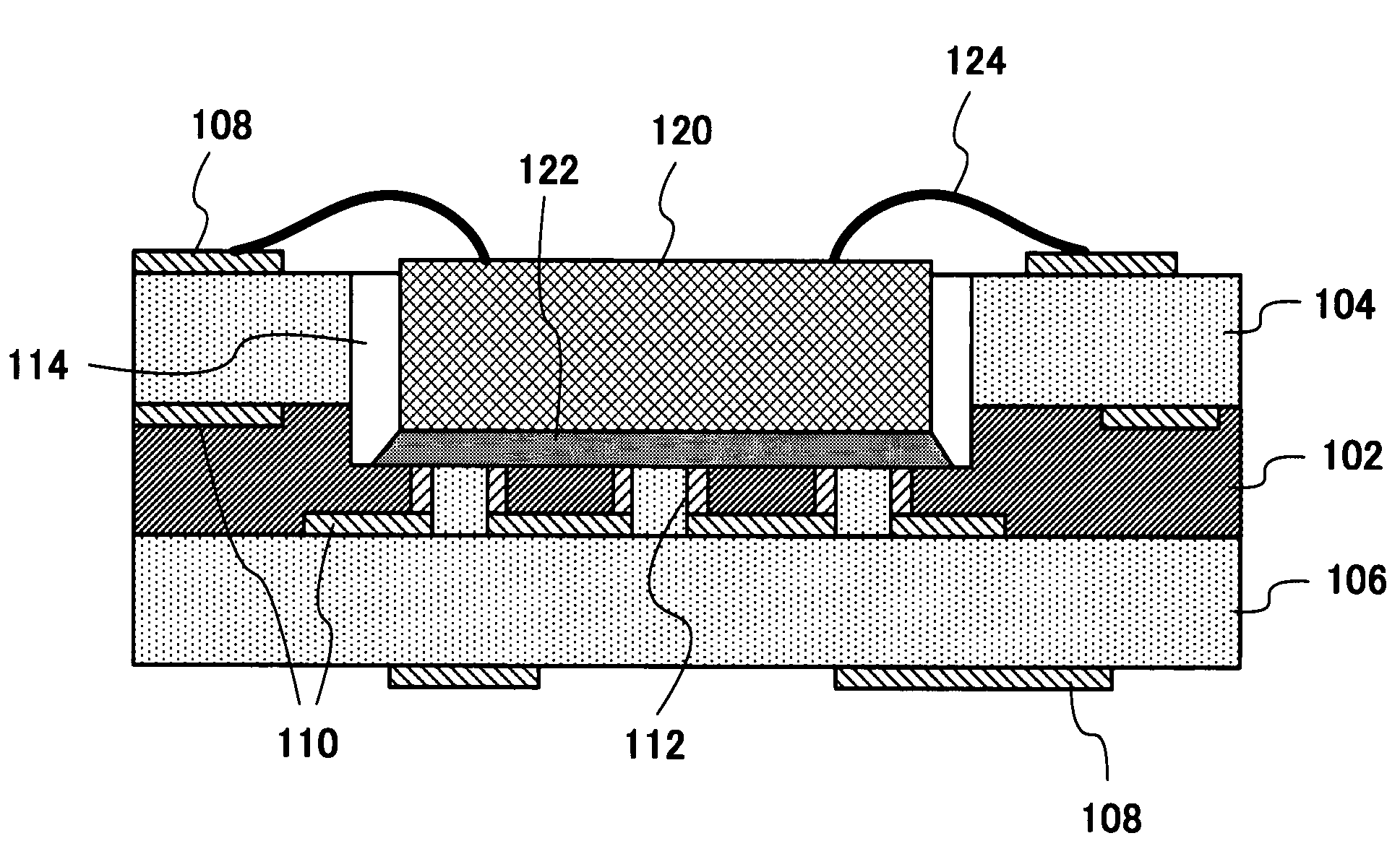
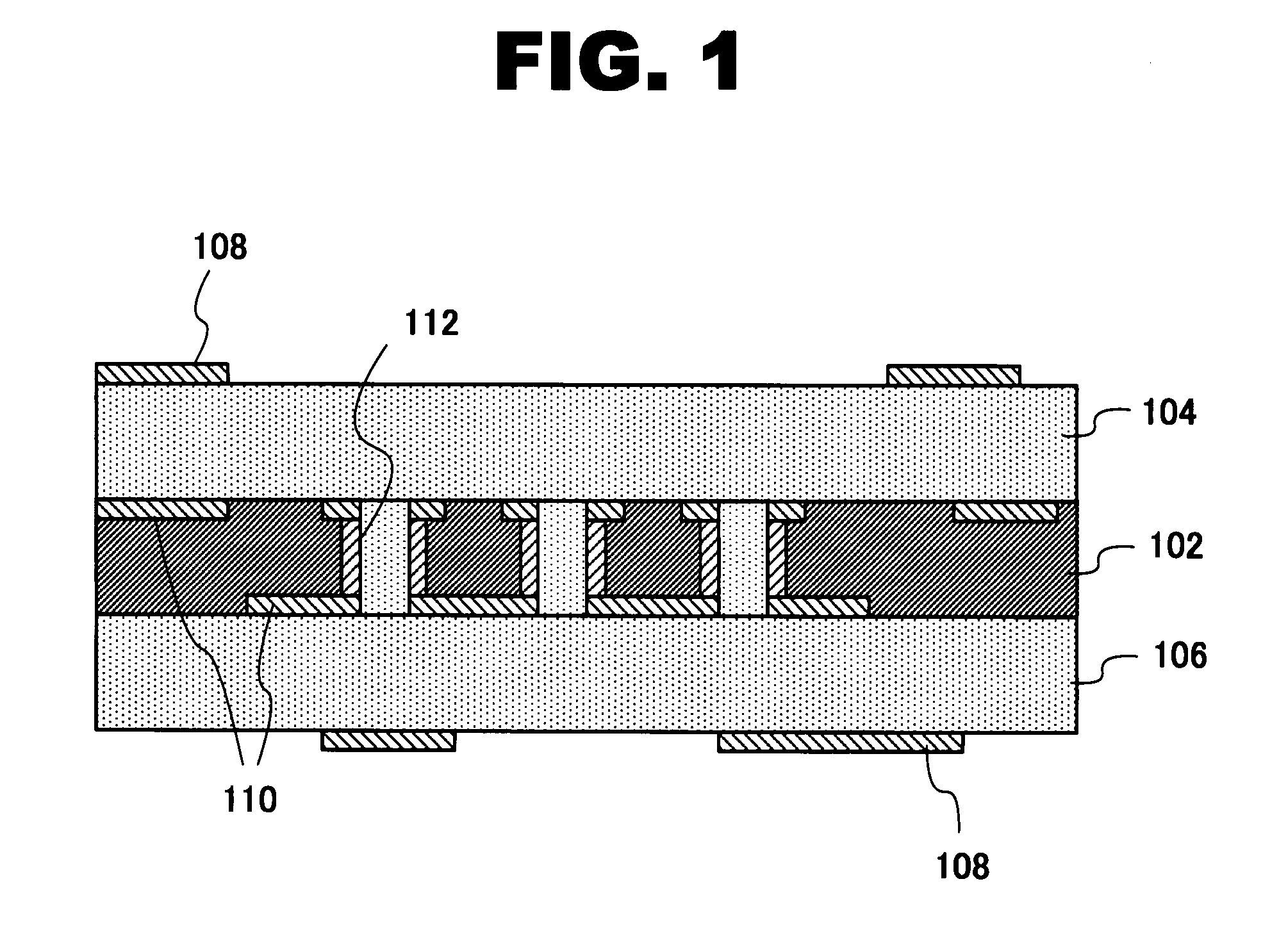
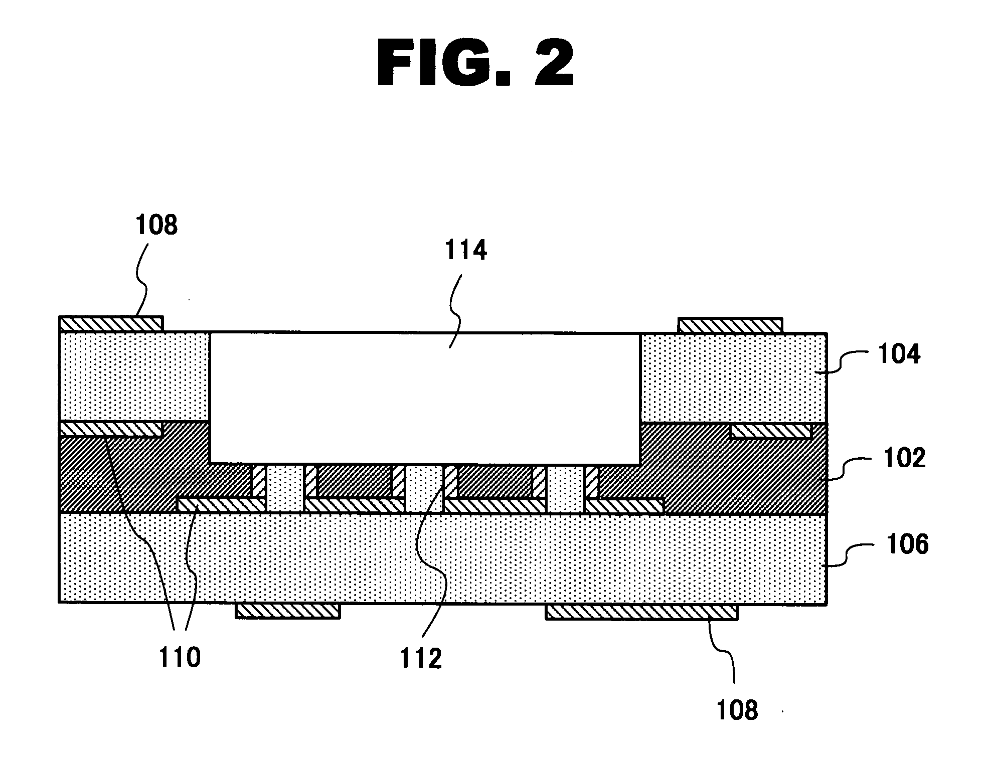
[0041]Preferred embodiments according to the present invention are illustrated in more details with reference to the attached drawings hereinafter. FIGS. 1, 2, and 4 are cross sectional views each showing a part of the manufacturing p...


PUM


Abstract

A semiconductor device that mounts a semiconductor chip in a multilayer substrate, including, inner layer conductive patterns formed in the multilayer substrate; extending conductive portions formed to extend on inner layer conductive patterns in the thickness direction, in the chip mounting area into which the semiconductor chip is mounted; and a cutout portion that is formed by cutting the multilayer substrate, and into which the semiconductor chip is contained, in the chip mounting area. And, in the cutout portion, the underside surface of the semiconductor chip and the inner layer conductive patterns are connected via the extending conductive portions at a same potential.

Description

CROSS REFERENCE TO RELATED APPLICATION[0001]This application claims the priority of Application No. 2006-266866, filed Sep. 29, 2006 in Japan, the subject matter of which is incorporated herein by reference.TECHNICAL FIELD OF THE INVENTION[0002]The present invention relates to a semiconductor device having a cutout structure and a method of manufacturing the same, in particular, to a semiconductor where a SOI (Silicon On Insulator) type semiconductor chip is mounted on a COB (Chip On Board) substrate, and a method of manufacturing the same.BACKGROUND OF THE INVENTION[0003]FIG. 8 and FIG. 9 are sectional views showing a part of manufacturing process of the prior-art semiconductor device. As shown in FIG. 8, in a multilayer substrate of the structure where a prepreg 2 is sandwiched between two core base materials 4, 6, inner layer conductive patterns 10 made of Cu are formed. Further, in the core base materials 4 and 6, blind via holes 30 are formed, and the insides thereof are filled...

Claims


Application Information

Patent Timeline
Patent Type & Authority Applications(United States)
IPC IPC(8): H01L23/48
CPCH01L23/13H01L23/49822H01L2924/15153H01L24/48H05K2201/10969H05K2201/09481H05K3/4697H05K3/4611H05K3/0044H01L23/50H01L2224/32225H01L2224/48091H01L2224/48227H01L2224/73265H01L2924/1517H05K1/183H01L2924/00014H01L2924/00012H01L24/73H01L2224/45099H01L2224/45015H01L2924/207
Inventor TAKAHASHI, NORIO
Owner LAPIS SEMICON CO LTD
Why Eureka
Try Eureka