Method of real time dynamic CD control

a real-time dynamic and control method technology, applied in the field of processing wafers, to achieve the effect of high metrology data density and high wafer throughpu

Inactive Publication Date: 2008-04-03
TOKYO ELECTRON LTD
View PDF4 Cites 20 Cited by
  • Summary
  • Abstract
  • Description
  • Claims
  • Application Information

AI Technical Summary

Benefits of technology

[0007]Embodiments of the invention provide a method of real time dynamic critical dimension (CD) control and optimization for a process of lithographically patterning resist coated wafers. The method provides the high metrology data density required for controlling and optimizing the patterning process, while allowing for high wafer throughput.

Problems solved by technology

In addition to the intended results, heat-treating may cause numerous problems.
For example, the light sensitive component of the photoresist may decompose at temperatures typically used to remove the solvent, which is an extremely serious concern for a chemically amplified resist (CAR) since the remaining solvent content has a strong impact on the diffusion and amplification rates.

Method used


Image

  • Method of real time dynamic CD control
  • Method of real time dynamic CD control
  • Method of real time dynamic CD control

Examples


Embodiment Construction

[0024]Embodiments of the invention provide a method for real time dynamic CD control and optimization associated with lithographically patterning resist coated wafers on a hotplate. The method provides high density CD metrology data collection for CD control and optimization while allowing high wafer throughput. According to one embodiment of the invention, the method includes constructing a CD metrology data map from CD metrology data obtained from test areas on the patterned wafers, where different groups of test areas are selected for two or more of the patterned wafers. Adjusted exposure and focus settings are established using the CD metrology data map to pattern additional resist coated wafers.

[0025]The terms “wafer” and “substrate” are used interchangeably herein to refer to a thin slice of material, such as a silicon crystal or glass material, upon which microcircuits are constructed, for example by diffusion, deposition, and etching of various materials.

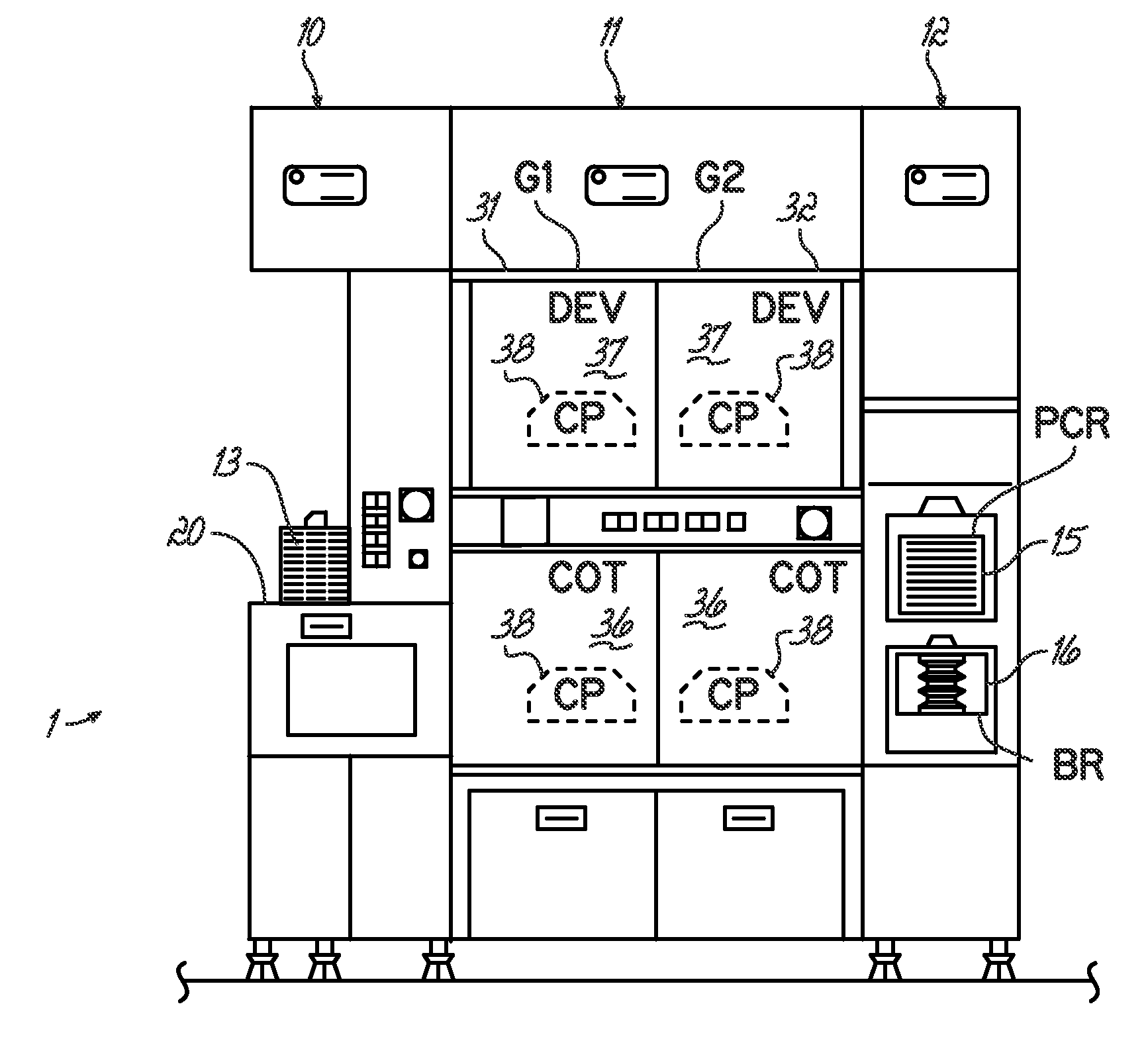
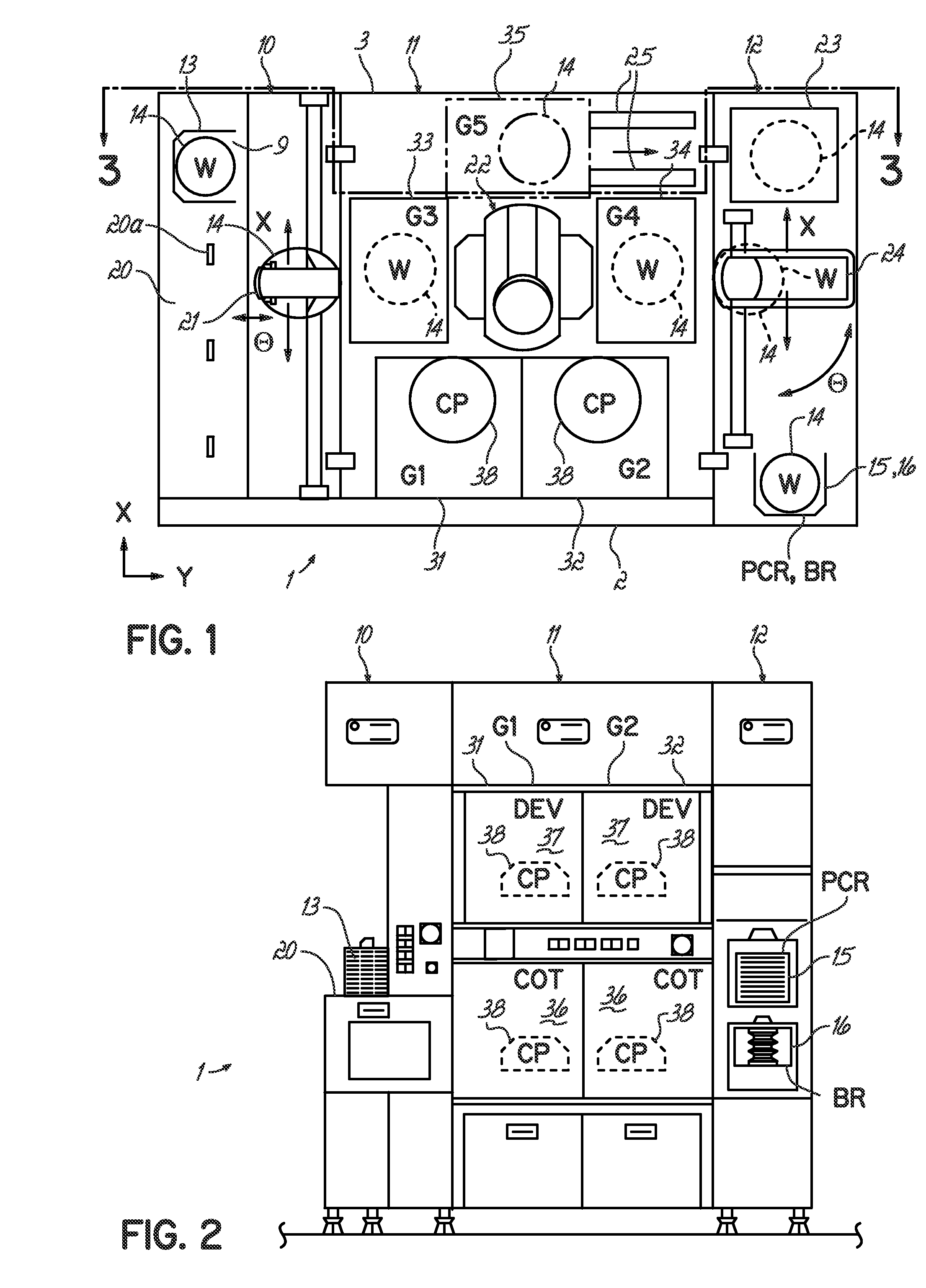
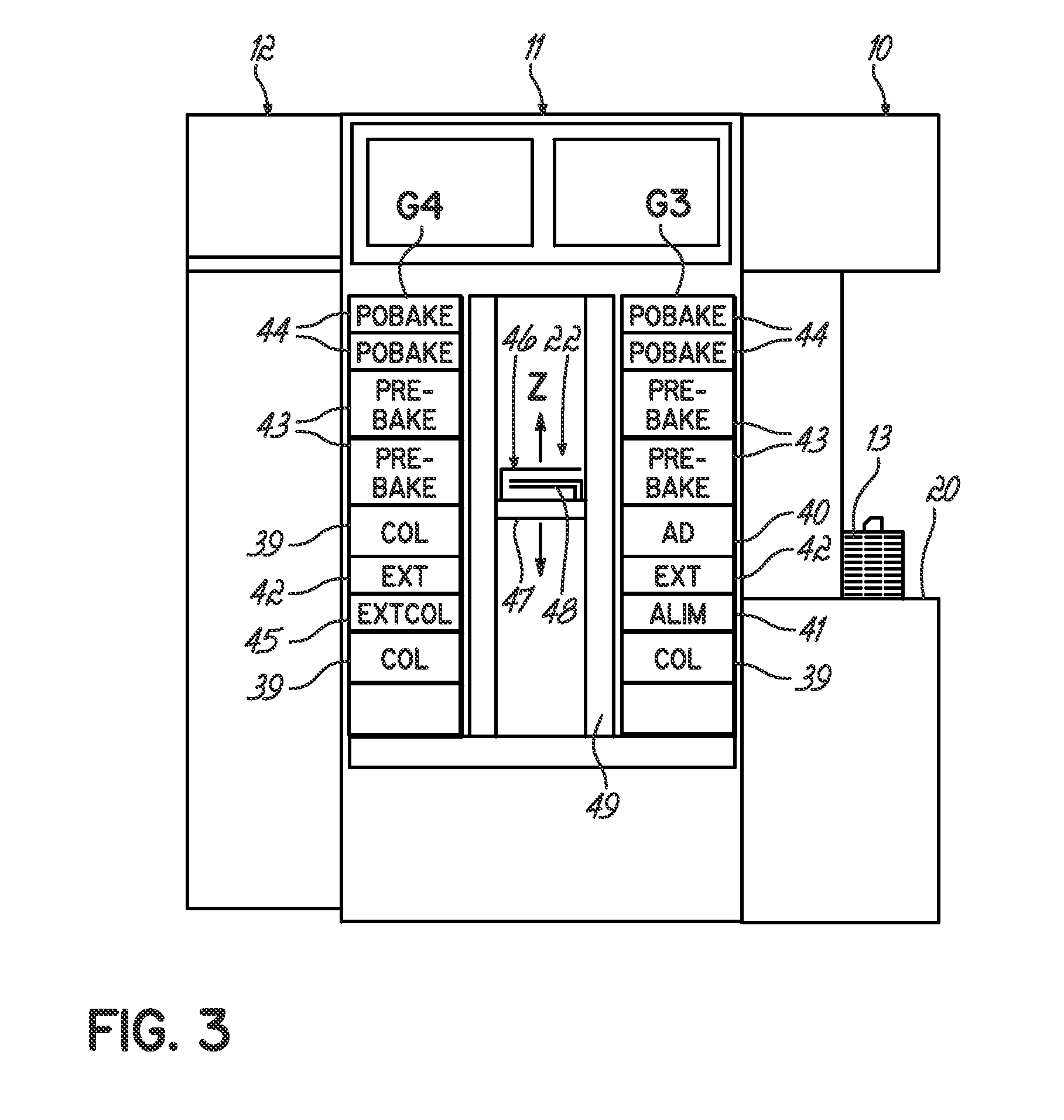
[0026]With reference...


PUM

PropertyMeasurementUnit
sizesaaaaaaaaaa
central anglesaaaaaaaaaa
wavelengthsaaaaaaaaaa

Abstract

A method of real time dynamic CD control in a system for patterning resist coated wafers. The method includes lithographically patterning the resist coated wafers using predetermined exposure dose and focus settings. The method further includes obtaining CD metrology data from test areas on the patterned wafers, where different groups of test areas are selected for two or more of the patterned wafers. A CD metrology data map is constructed using the CD metrology data, adjusted exposure dose and/or focus settings are established using the CD metrology data, and additional wafers are then patterned.

Description

CROSS-REFERENCE TO RELATED APPLICATIONS[0001]This application is related to co-pending U.S. patent application Ser. No. 11 / 536,991 (Attorney Docket No. TTCA-009A), entitled “METHOD OF REAL TIME DYNAMIC CD CONTROL,” filed on even date herewith, the entire content of which is hereby incorporated by reference.FIELD OF THE INVENTION[0002]The invention relates to a method for processing wafers, and more particularly, to a method of real time dynamic critical dimension (CD) control and optimization for lithographically patterned wafers.BACKGROUND OF THE INVENTION[0003]In a photolithography process for manufacturing semiconductor devices and liquid crystal displays (LCD's), resist is coated on a substrate, and the resultant photoresist coating film is exposed to light and developed. The series of processing stages are carried out in a coating / developing processing system having discrete heating sections, such as a prebaking unit and a postbaking unit. Each heating section incorporates a ho...

Claims


Application Information

Patent Timeline
Patent Type & Authority Applications(United States)
IPC IPC(8): G01N21/00
CPCG01N21/4788G03F7/70625G03F7/70558
Inventor SCHEER, STEVEN
Owner TOKYO ELECTRON LTD
Why Eureka
Try Eureka