Integrated circuit device including a circuit to generate error correction code for correcting error bit for each of memory circuits

Inactive Publication Date: 2008-04-03
KK TOSHIBA
View PDF6 Cites 7 Cited by
  • Summary
  • Abstract
  • Description
  • Claims
  • Application Information

AI Technical Summary

Benefits of technology

[0009]According to a first aspect of the present invention, there is provided an integrated circuit device comprising a plurality of memory circuits which store data, a plurality of code generating circuits which are provided for the memory circuits, respectively, to generate an error correction code to correct an error bit of each data stored in the memory circuits, at least one code storage memory which is shared by the memory circuits to store code data obtained by the error correction code, at least one decoding circuit which is provided for each of the memory circuits to detect the error bit based on the cod

Problems solved by technology

As the semiconductor circuit components (semiconductor chips) of a semiconductor integrated circuit have decreased in size, soft errors have recently been caused.
In particular, data in a memory chip appears here and there and thus becomes a problem.
In the near future, soft errors will increase with the decrease of electr

Method used


Image

  • Integrated circuit device including a circuit to generate error correction code for correcting error bit for each of memory circuits
  • Integrated circuit device including a circuit to generate error correction code for correcting error bit for each of memory circuits
  • Integrated circuit device including a circuit to generate error correction code for correcting error bit for each of memory circuits

Examples


Example

First Embodiment

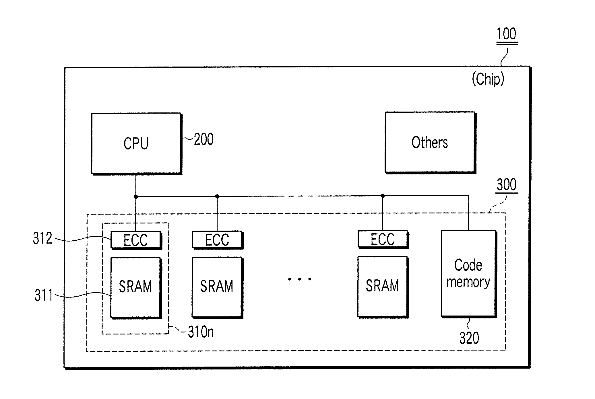
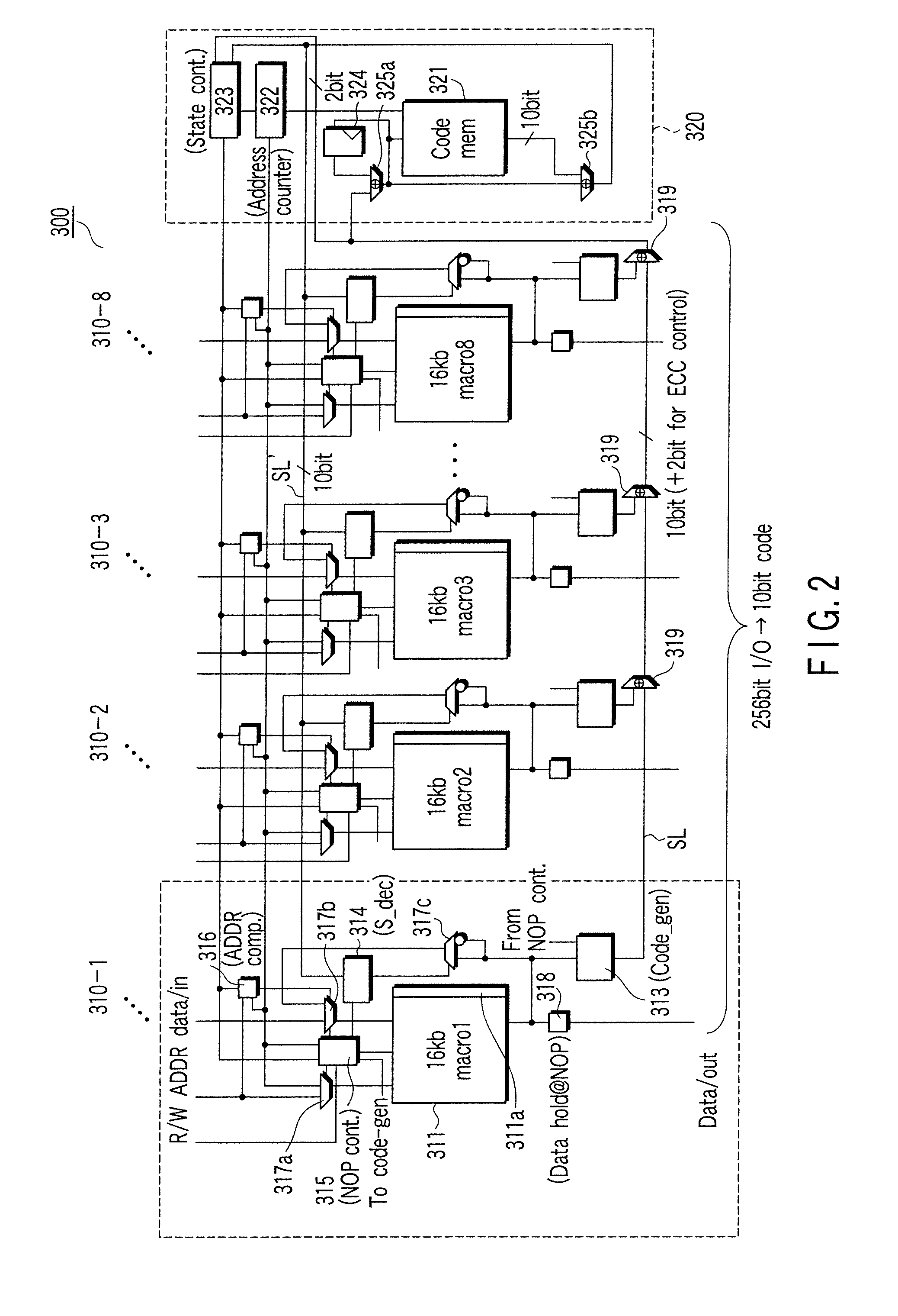
[0035]FIG. 1 shows a basic configuration of an integrated circuit device according to a first embodiment of the present invention. The first embodiment will be described taking as an example a semiconductor integrated circuit in which a plurality of semiconductor circuit components (semiconductor chips) are integrated in one package (single chip). In the semiconductor integrated circuit, a partial code generating / decoding circuit (peripheral circuit) for ECC is provided for each small-capacity memory chip (memory macro). Bit errors in each memory macro can thus be corrected at once in data read operation. In the first embodiment, the size (capacity or memory configuration corresponding to the number of addresses=the number of words×bit width) of memory macros is the same.

[0036]Referring to FIG. 1, the semiconductor integrated circuit of the first embodiment includes a plurality of semiconductor circuit components, such as a central processing unit (CPU) 200 and an EC...

Example

Second Embodiment

[0088]FIG. 9 shows an arrangement (address space) of an ECC memory circuit in an integrated circuit device according to a second embodiment of the present invention. The second embodiment is directed to the semiconductor integrated circuit of the first embodiment which is so configured that data stored in a plurality of memory macros whose sizes are different (but whose word widths are the same) can be corrected at once. The same components as those of the first embodiment are denoted by the same reference numerals and their detailed descriptions are omitted.

[0089]In the second embodiment, as shown in FIG. 9, eighteen memory circuit units 310 in all are prepared for an ECC memory circuit 300a. Of the eighteen memory circuit units 310, eight memory circuit units 310 each have a memory macro 311-1a whose capacity (memory structure) is 128 kb (32 bits×4 Kword). Other eight memory circuit units 310 each have a memory macro 311-1b whose capacity (memory structure) is 256...

Example

Third Embodiment

[0093]FIG. 10 shows a basic arrangement of an ECC memory circuit in an integrated circuit device according to a third embodiment of the present invention. The third embodiment is directed to the semiconductor integrated circuit of the first embodiment which is so configured that data stored in memory macros whose sizes are different or whose word widths are the same can be corrected at once. The same components as those of the first embodiment are denoted by the same reference numerals and their detailed descriptions are omitted.

[0094]In the third embodiment, as shown in FIG. 10, five memory circuit units 310-1, 310-2, 310-3, 310-4 and 310-5 in all are prepared for an ECC memory circuit 300b. Of these five memory circuit units, four memory circuit units 310-1, 310-2, 310-3 and 310-4 each have a memory macro 311-1d whose capacity (memory structure) is 32 kb (32 bits×1K words). In contrast, the memory circuit unit 310-5 each have a memory macro 311-1a whose capacity (m...


PUM


Abstract

An integrated circuit device includes a plurality of memory circuits, a memory hibernation state control circuit to bring the memory circuits into a hibernation state in response to an external command, a state controller which indicates an interrupt in a memory circuit in a hibernation state, and a plurality of partial ECC code generating circuits which are provided for the memory circuits, respectively, to code hold data of an address of a memory circuit in a hibernation state in accordance with a rule of a Hamming code determinant by an interrupt in the memory circuit in the hibernation state. The integrated circuit device further includes a code storage memory which obtains ECC code data corresponding to all of the hold data based on partial ECC codes coded by the partial ECC code generating circuit and stores the ECC code data in a corresponding address.

Description

CROSS-REFERENCE TO RELATED APPLICATIONS[0001]This application is based upon and claims the benefit of priority from prior Japanese Patent Application No. 2006-268072, filed Sep. 29, 2006, the entire contents of which are incorporated herein by reference.BACKGROUND OF THE INVENTION[0002]1. Field of the Invention[0003]The present invention relates to an integrated circuit device. More specifically, the invention relates to a semiconductor integrated circuit having an error checking and correcting (ECC) function within a single chip or on a single printed circuit board and an integrated circuit system having the same function.[0004]2. Description of the Related Art[0005]As the semiconductor circuit components (semiconductor chips) of a semiconductor integrated circuit have decreased in size, soft errors have recently been caused. It is considered that the soft errors are caused by alpha rays emitted from an isotope in a package and neutrons coming from space. In particular, data in a m...

Claims


Application Information

Patent Timeline
IPC IPC(8): H03M13/00
CPCH03M13/19G06F11/1044
Inventor KUSHIDA, KEIICHI
Owner KK TOSHIBA
Why Eureka
Try Eureka