Method for fabricating a semiconductor device, method for fabricating an electronic device, and semiconductor fabricating apparatus

a semiconductor and electronic technology, applied in the direction of electrical devices, liquid surface applicators, coatings, etc., can solve the problems of poor mass production characteristics, large dispersion of element characteristics, and high equipment costs, so as to improve the uniformity of the thermal process

Inactive Publication Date: 2008-04-17
SEIKO EPSON CORP
View PDF27 Cites 13 Cited by
  • Summary
  • Abstract
  • Description
  • Claims
  • Application Information

AI Technical Summary

Benefits of technology

[0024]For example, a nozzle having an approximately linear orifice is provided below the plurality of flames, and the plurality of flames are emitted through the orifice. This configuration improves the uniformity of the thermal process by emitting a flame from an approximately linear orifice of the nozzle.
[0025]For example, the moving unit controls movement in...

Problems solved by technology

In methods of solid phase growth by the above thermal process, the substrate is subject to a large thermal load which may easily cause warping and cracking of the substrate because the substrate is heated to a high temperature between 600 and 1,000° C. Furthermore, mass production characteristics are poor because a long time is needed for crystallization....

Method used


Image

  • Method for fabricating a semiconductor device, method for fabricating an electronic device, and semiconductor fabricating apparatus
  • Method for fabricating a semiconductor device, method for fabricating an electronic device, and semiconductor fabricating apparatus
  • Method for fabricating a semiconductor device, method for fabricating an electronic device, and semiconductor fabricating apparatus

Examples


Embodiment Construction

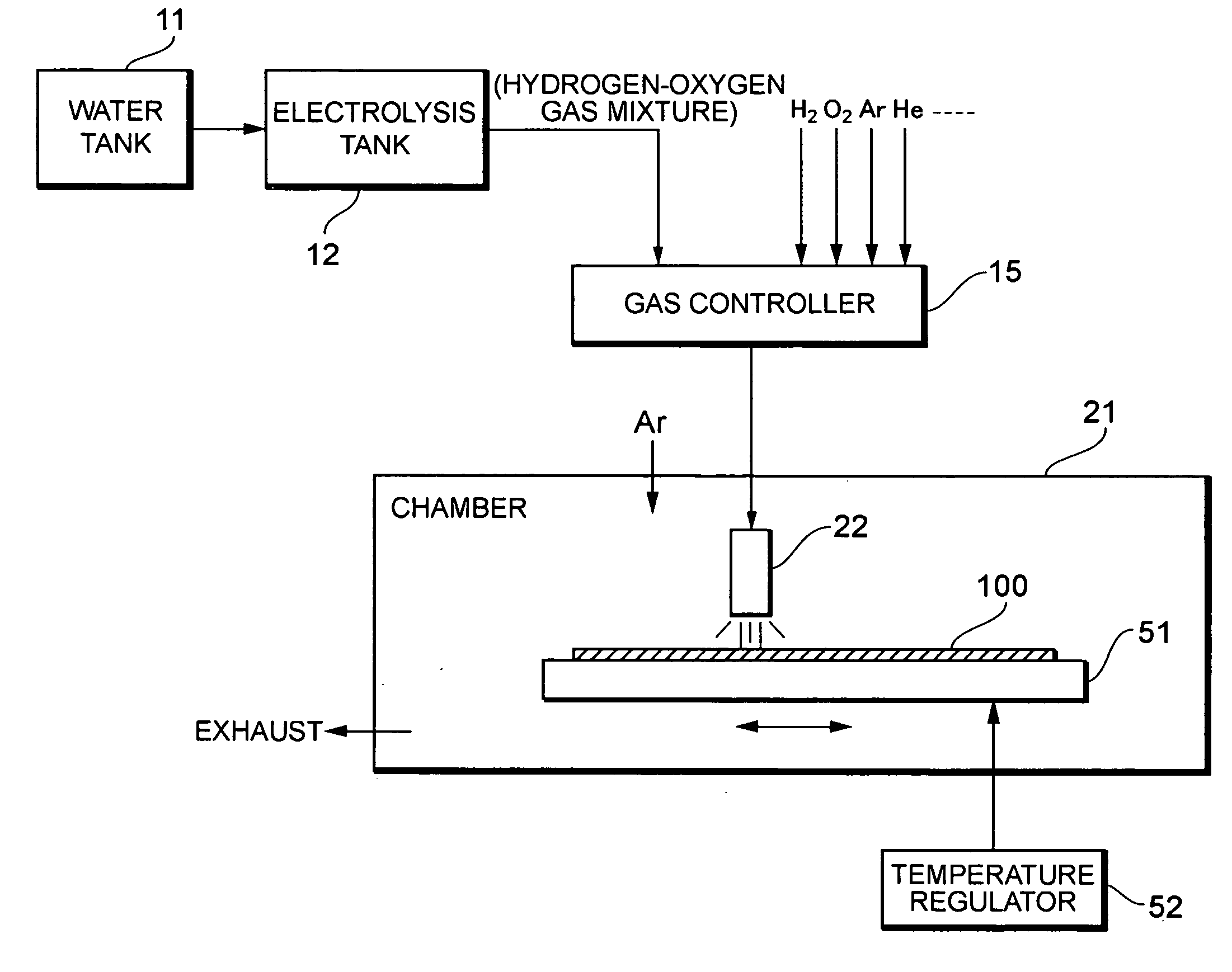
[0048]In the present embodiment, thermal processing is performed on a film on a substrate using a hydrogen and oxygen gas mixture as a fuel. This thermal process is referred to as the hydrogen flame process hereinafter. Furthermore, the flame of the gas burner is referred to as the hydrogen flame. This thermal process is performed, for example, when recrystallizing a silicon film (semiconductor film, semiconductor layer).

[0049]The embodiments of the present invention are described hereinafter with reference to the figures. Parts having like functions are designated by like reference numbers, and repetitious description is omitted.

[0050]Semiconductor Fabricating Apparatus

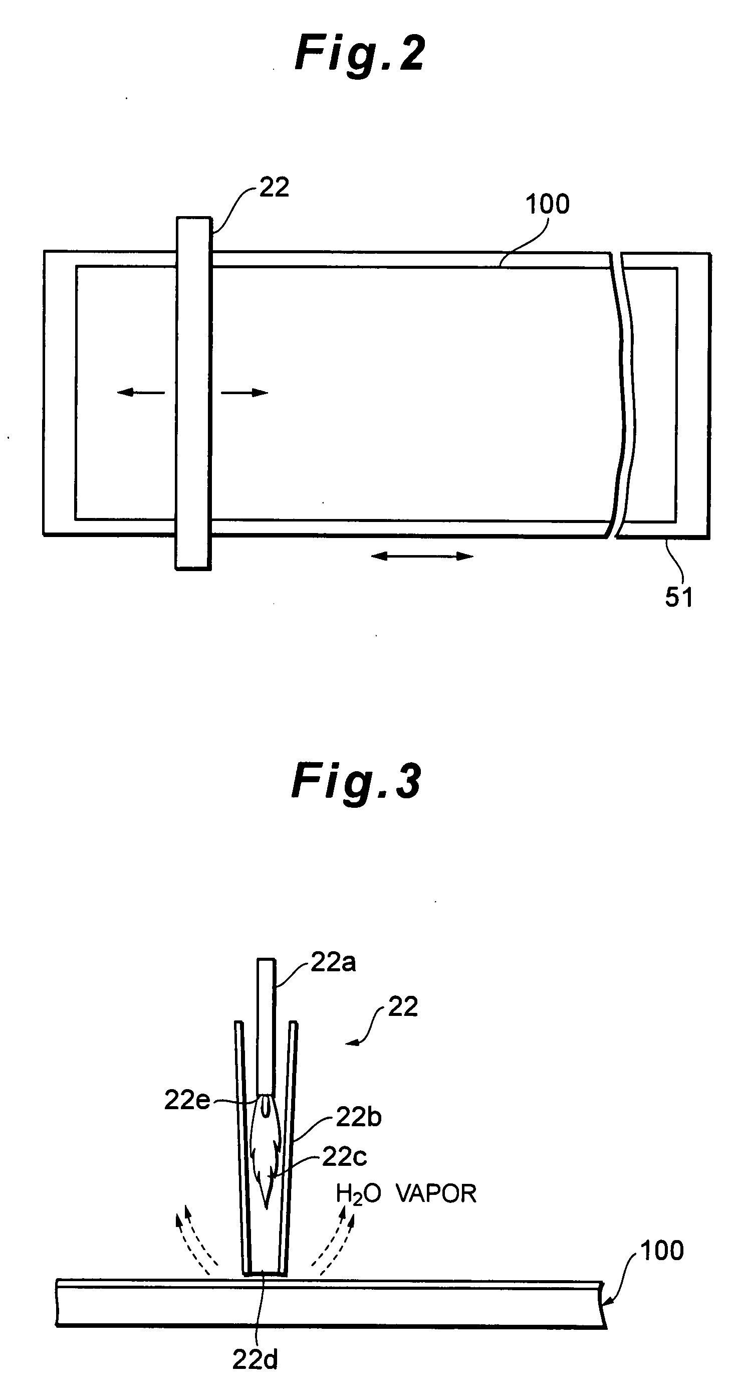
[0051]A semiconductor fabricating apparatus used to fabricate the semiconductor device of the present embodiment is described hereinafter with reference to FIGS. 1 through 9.

[0052]FIG. 1 shows a structural example of the semiconductor fabricating apparatus (semiconductor element fabricating apparatus) used to fabrica...


PUM


Abstract

A method for fabricating a semiconductor device including: a step of forming a first film on a substrate; and a step of performing a thermal process by scanning the first film with a flame of a gas burner using a hydrogen and oxygen gas mixture as a fuel, wherein the flame of the gas burner is approximately linear.

Description

CROSS-REFERENCES TO RELATED APPLICATIONS[0001]The entire disclosure of Japanese Patent Application No. 2006-277956, filed on Oct. 11, 2006 is expressly incorporated by reference herein.BACKGROUND[0002]1. Technical Field[0003]The present invention relates to a method for fabricating a semiconductor device particularly to improving the uniformity of the thermal processing temperature during a thermal processing step.[0004]2. Related Art[0005]Crystallization methods designed to recrystallize silicon formed as a film on a substrate using a CVD (chemical vapor deposition) method include solid phase growth utilizing a process of high temperature heating at 600 to 1,000° C., laser annealing methods utilizing excimer laser emission, thermal plasma jet methods utilizing thermal plasma as a heat source and the like (JP-A-11-145148; Crystallization of Si Thin Film Using Thermal Plasma Jet and Its Application to Thin-Film Transistor Fabrication, S. Higashi, AM-LCD '04 Technical Digest Papers, p...

Claims


Application Information

Patent Timeline
IPC IPC(8): B05C11/00H01L21/477
CPCH01L21/02532H01L21/02667H01L21/67103H01L21/67098H01L21/02691H01L21/324
Inventor SATO, MITSURUUTSUNOMIYA, SUMIO
Owner SEIKO EPSON CORP
Why Eureka
Try Eureka