Substrate with surface finished structure and method for making the same

a surface finished and surface technology, applied in the direction of resist details, printed circuit aspects, non-metallic protective coating applications, etc., can solve the problems of osp still volatilizing to lose the protection of copper surface, molten solder cannot be mounted, affecting the quality of telecommunication, etc., to prevent the oxidation of the solder pad

a surface finished and surface technology, applied in the direction of resist details, printed circuit aspects, non-metallic protective coating applications, etc., can solve the problems of osp still volatilizing to lose the protection of copper surface, molten solder cannot be mounted, affecting the quality of telecommunication, etc., to prevent the oxidation of the solder pad

US20080093109A1Inactive Publication Date: 2008-04-24PHOENIX PRECISION TECH CORP

Image

  • Substrate with surface finished structure and method for making the same
  • Substrate with surface finished structure and method for making the same
  • Substrate with surface finished structure and method for making the same

Examples


Embodiment Construction

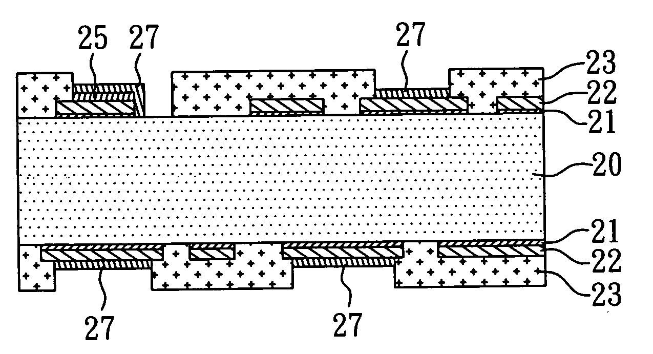
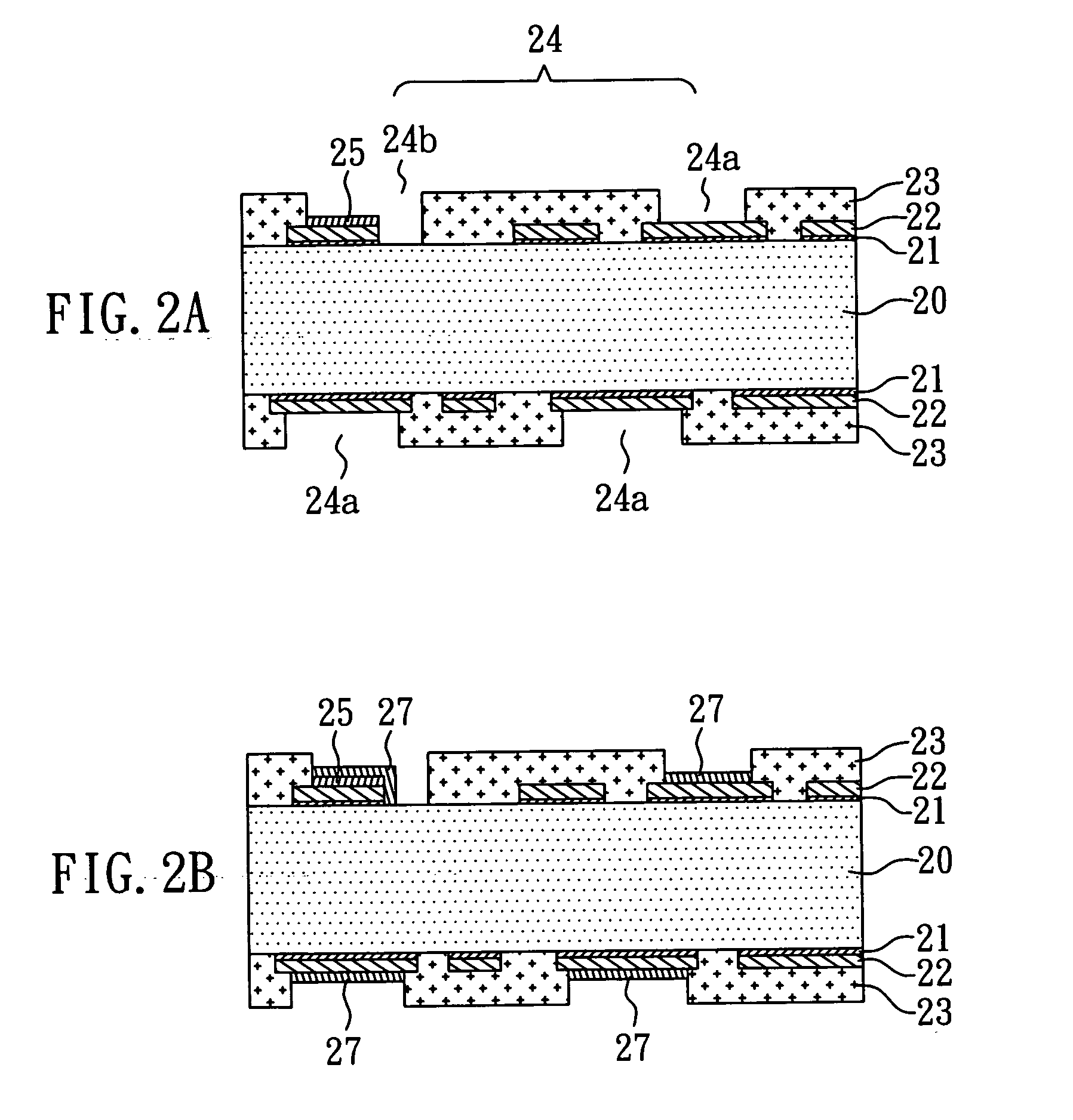
[0028]Referring to FIGS. 2A to 2B, which are schematic cross-section illustrations of the substrate with surface finished structure of a preferred embodiment of the present invention. First, as shown in FIG. 2A, a substrate 20 is provided, which can be a single-layer or a multi-layer finished the preceding process circuit board. Besides, a seed layer 21, a circuit layer 22, and a solder mask 23 for isolation and protection are formed on the upper and lower surface of the substrate 20, and a plurality of openings are formed in the solder mask 23 by exposure and development to expose the portion of the circuit layer 22 therebeneath to be electrical contact pads 24, wherein the electrical contact pads 24 comprise at least a wire bonding pad 24b and solder pads 24a (step A). Then, a Ni / Au layer 25 is formed on the surface of the wire bonding pad 24b (a Ni layer is formed first, and then an Au layer is covered thereon) (step B).

[0029]After that, as shown in FIG. 2B, a chemical gold layer...


PUM


Abstract

A substrate with surface finished structure and a method for manufacturing the same are disclosed. The method comprises: forming a circuit layer and a solder mask on the surface of the substrate in sequence, wherein a plurality of openings are formed in the solder mask to expose the portion of the circuit layer to be electrical contact pads which having at least a wire bonding pad and a plurality of solder pads; and forming a Ni / Au layer on the surface of the wire bonding pad and a chemical gold layer on the surface of the solder pads. Therefore, the disclosed structure can prevent the electrical contact pads from oxidation for a long time.

Description

BACKGROUND OF THE INVENTION[0001]1. Field of the Invention[0002]The present invention relates to a surface with surface finished structure and a method for making the same and, more particularly, to a surface with surface finished structure and a method for manufacturing the same that apply to a chemical gold layer is formed on the surface of the electrical contact pads.[0003]2. Description of Related Art[0004]Generally speaking, to prevent further oxidation of the electrical pads on the substrate, the surface of the electrical pads are surface-treated by coating a layer of organic solderability preservatives (i.e. OSP) for inhibiting oxidation and extending the waiting time for surface finished process. If the substrate is not subject to the surface treatment illustrated above, the copper in the electrical contact pads will be easily oxidized to produce a metal oxide layer after a period of time. As a result, for the molten solders to stick on, the surface of the metal oxide layer ...

Claims


Application Information

Patent Timeline
24 Apr 2008
Publication
US20080093109A1
IPC
H05K1/00
CPC
H05K3/243; H05K3/28; H05K2203/0574; H05K2203/049; H05K2201/0391
Inventors
HSU, SHIH-PING; YEN, YA-LUN