Semiconductor device

a semiconductor and device technology, applied in the field of semiconductor devices, can solve the problems of inability to easily switch the semiconductor device the operation mode cannot be changed, and the semiconductor device cannot be easily changed to the test mode, etc., to achieve the effect of suppressing the increase in the circuit scale and the chip area

Inactive Publication Date: 2008-04-24
ELPIDA MEMORY INC
View PDF0 Cites 12 Cited by
  • Summary
  • Abstract
  • Description
  • Claims
  • Application Information

AI Technical Summary

Benefits of technology

[0015]The present invention has been made in view of the foregoing problems, and an object of the present invention is to provide a semiconductor device in which function modes of the semiconductor device can be changed without difficulty and failure analysis can be conducted in an apparatus in which the semiconductor device is mounted.
[0024]This can suppress increases in the circuit scale and the chip area when the function modes of the semiconductor device are switched for failure analysis, as compared with conventional anti-fuses.
[0025]In addition, in accordance with the present invention, the semiconductor device does not suffer damage due to dissolution of resin with a solvent, unlike conventional bonding options, and the software of the apparatus does not have to be modified.

Problems solved by technology

However, the semiconductor device disclosed in Patent Document 1 has a problem in that the semiconductor device is fixed to any one of a group of operation modes when it is shipped and thereafter it is not possible to change the semiconductor device from the fixed operation mode to a different operation mode.
Moreover, the semiconductor devices disclosed in Patent Documents 2 and 3 have a problem in that, once the operation modes of the semiconductor devices are fixed, the operation modes cannot be changed since the anti-fuse is an irreversible conversion component.
Furthermore, in some cases, there may be a need to test semiconductor devices with their function switched, e.g., their internal power supply voltages, delay values of signals, or the like changed, for failure analysis.
However, if it is determined that the semiconductor device is defective after it is mounted in an apparatus, the semiconductor device cannot be easily switched to the test mode unlike the test using the tester.
This may cause the semiconductor device to be damaged, which may lead to circuit analysis becoming impossible due to circuit breakage in some cases.
Moreover, in the semiconductor devices as disclosed in Patent Documents 2 and 3, the function of the semiconductor devices can only be changed once, and thus cannot be used for failure analysis.
However, it is difficult or almost impossible to do so because the software in the apparatus is produced by a customer.

Method used


Image

  • Semiconductor device
  • Semiconductor device
  • Semiconductor device

Examples


first embodiment

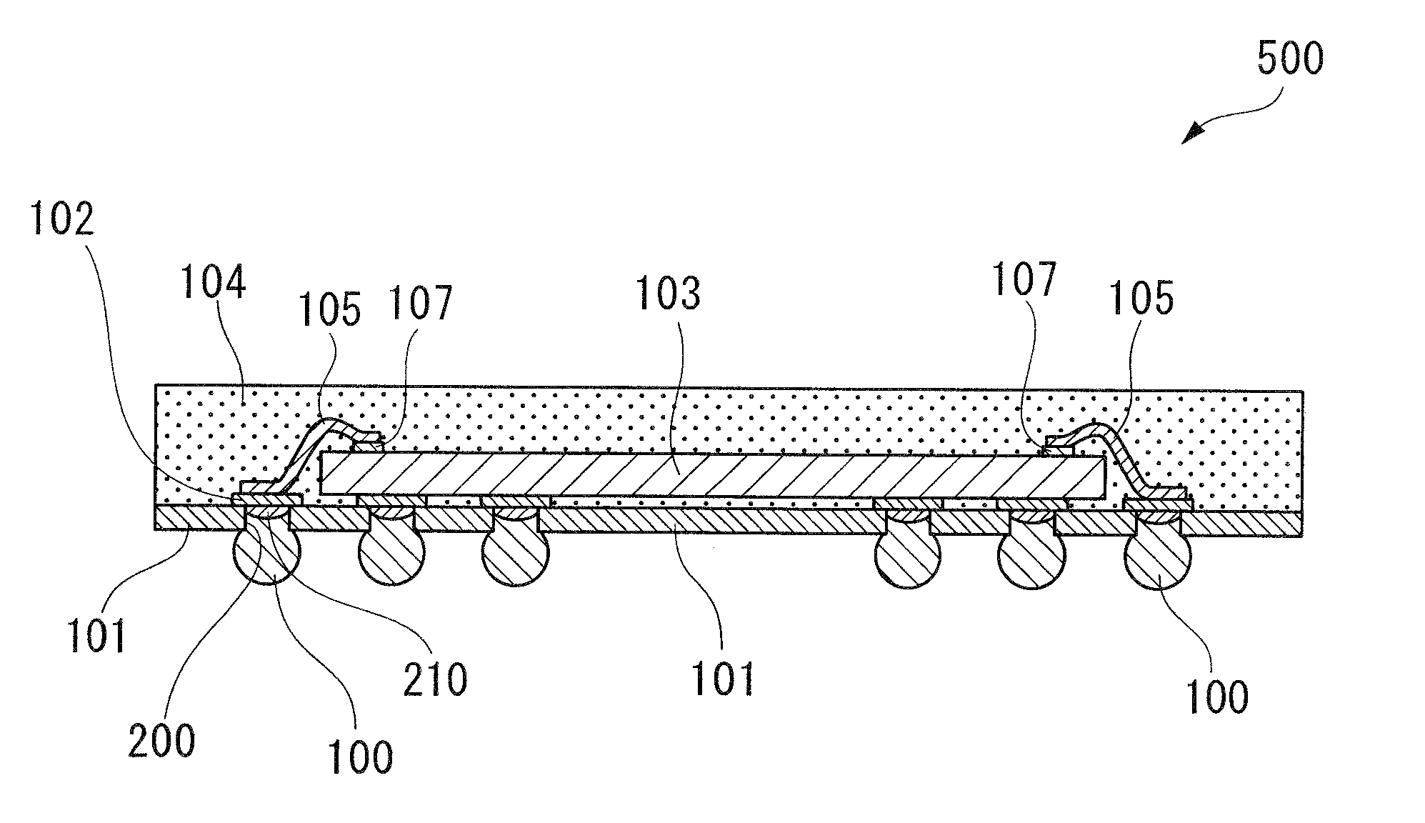
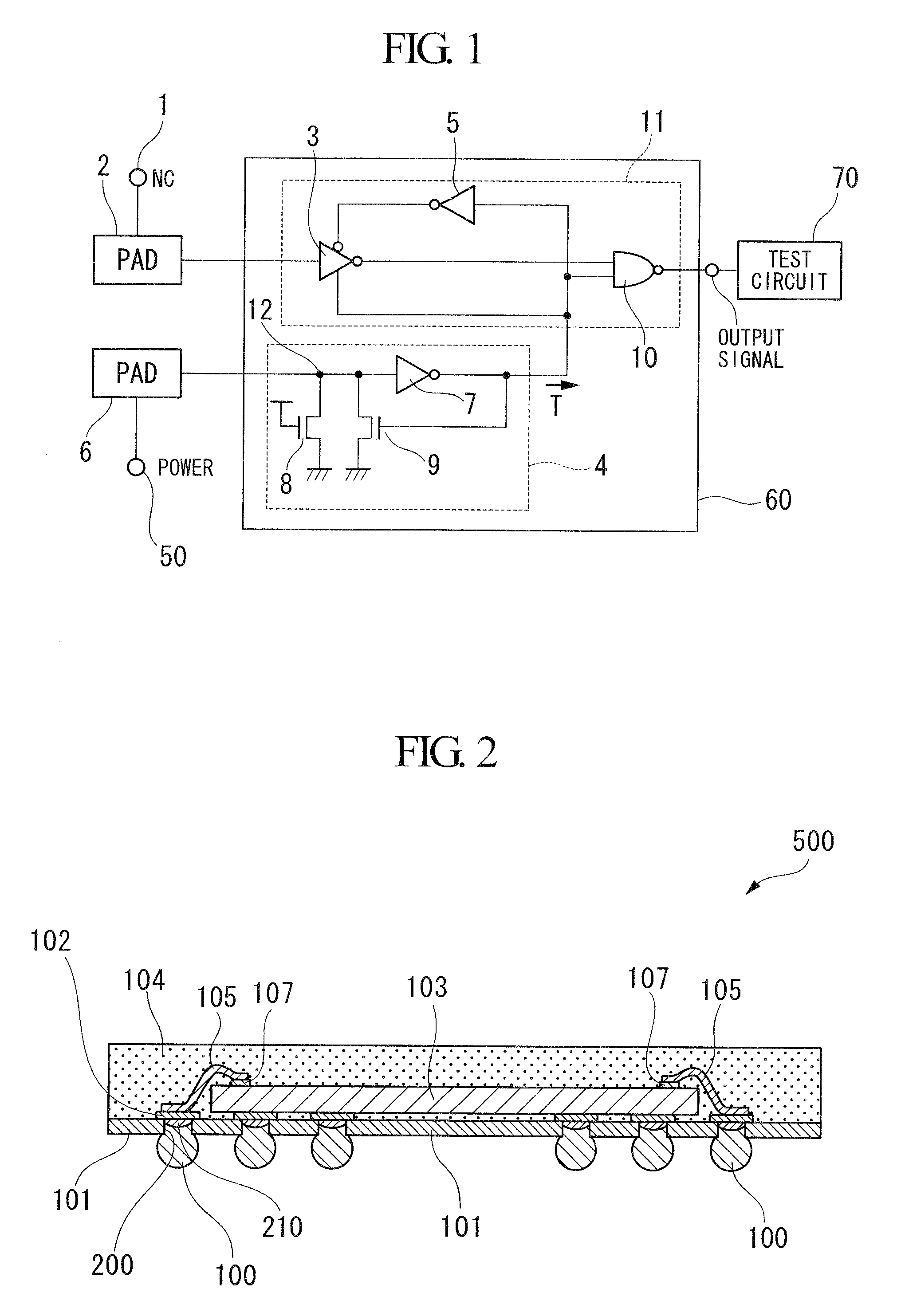
[0038]FIG. 1 is a block diagram showing an exemplary configuration of a mode switching unit 60 provided in a semiconductor chip 103 (see FIG. 2) in a semiconductor device 500 (see FIG. 2) in accordance with a first embodiment of the present invention.

[0039]Referring to FIG. 1, the mode switching unit 60 includes a mode detector 4 and a mode selector 11. An output signal of the mode switching unit 60 is supplied to a test circuit 70.

[0040]The mode detector 4 includes n channel type MOS (metal oxide semiconductor) transistors (hereinafter abbreviated as transistors) 8 and 9 and an inverter (inverting circuit) 7.

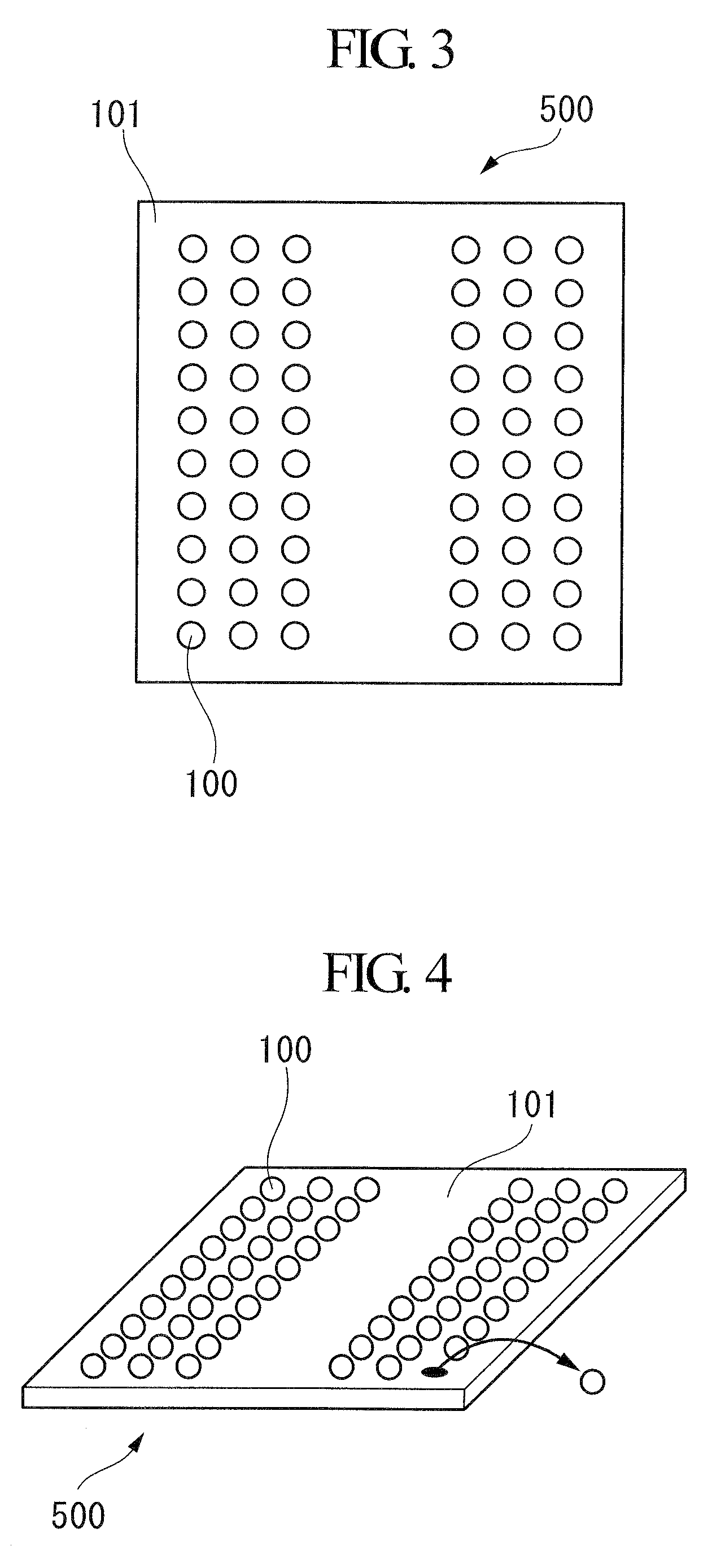
[0041]A pad (hereinafter also referred to as a detection pad) 6, which is a lead-out electrode formed on the semiconductor chip 103, is connected via a boding wire (corresponding to a bonding wire 105 of FIG. 2) to a via hole (corresponding to a via hole 200 shown in FIG. 2, hereinafter referred to as external power supply via holes) to which power is supplied from the outside ...

second embodiment

[0086]Next, a process of switching a plurality of function modes of the semiconductor chip 103 depending on the presence or absence of a solder ball in the same way as the first embodiment will be described.

[0087]For example, in the case of card type electronic devices, there is a need to prepare separate semiconductor chips in compliance with respective specifications, such as command systems to control an internal circuit 90 (FIG. 7), since the command systems are different from each other even when the specifications of the command transfer protocol are the same.

[0088]To meet such a need, semiconductor chips for card type electronic devices which can deal with different command systems (for example, both of a command system A and a command system B) are prepared.

[0089]In addition, like the first embodiment, a detection via hole and a detection pad are provided, and the internal circuit 90 switches the command systems depending on whether or not a solder ball is mounted. That is, ...


PUM


Abstract

A semiconductor device is provided in which function modes thereof can be changed without difficulty and failure analysis can be conducted in an apparatus in which the semiconductor device is mounted. A semiconductor device uses a ball grid array package and includes: a semiconductor chip that is provided within the semiconductor device and has a pad; a detection via hole connected to the pad; a solder ball that is attachable to and detachable from the detection via hole and connects or disconnects a power supply electrode of a substrate on which the semiconductor device is mounted and the detection via hole in correspondence to attachment or detachment of the solder ball to or from detection via hole, respectively; and a mode switching unit that detects a voltage level of the pad connected to the detection via hole and switches function modes in the semiconductor device depending on the voltage level.

Description

BACKGROUND OF THE INVENTION[0001]1. Field of the Invention[0002]The present invention relates to a semiconductor device which is capable of switching between a plurality of function modes provided therein.[0003]Priority is claimed on Japanese Patent Application No. 2006-288727, filed Oct. 24, 2006, the contents of which are incorporated herein by reference.[0004]2. Description of Related Art[0005]In the related art, there are semiconductor devices which are fixed to one of two operation modes when they are shipped.[0006]Examples of such semiconductor devices may include a semiconductor device which selects one of two operation modes depending on whether to bond a pin to a lead wire, to which a power supply voltage is applied, using a bonding option (for example, see Japanese Unexamined Patent Application, First Publication No. 2004-47720 (hereinafter referred to as “Patent Document 1”)).[0007]In addition, there are semiconductor devices which select one of two operation modes using ...

Claims


Application Information

Patent Timeline
Patent Type & Authority Applications(United States)
IPC IPC(8): H01L23/58G01R31/02
CPCG01R31/2884H01L22/32H01L2924/3011H01L2224/48227H01L2224/48472H01L2224/73265H01L2924/15311H01L2924/13091H01L2924/00
Inventor KIYOTA, GORO
Owner ELPIDA MEMORY INC
Why Eureka
Try Eureka