
Predictive duty ratio generating circuit and method for synchronous boost converters operating in PFM mode

a technology of generating circuit and generating circuit, which is applied in the direction of electric variable regulation, process and machine control, instruments, etc., can solve the problems of increasing power loss, reducing overall efficiency, and not well suited circuit structure for low voltage designs

Active Publication Date: 2008-04-24
TEXAS INSTR INC
View PDF8 Cites 49 Cited by
  • Summary
  • Abstract
  • Description
  • Claims
  • Application Information

AI Technical Summary

Benefits of technology

[0011]It is an object of the invention to provide a very accurate synchronous DC-to-DC boost converter which avoids transfer of charge back into an input signal source when the direction of the inductor current changes.
[0012]It is another object of the invention to provide a very accurate synchronous DC-to-DC boost converter that can detect and / or prevent reversed inductor current without requiring the use of an expensive, fast, precise comparator.
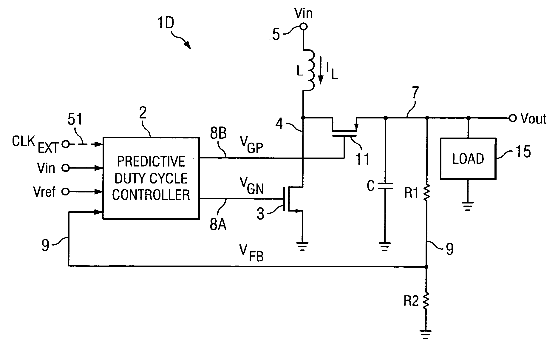
[0014]In one embodiment, the invention provides a synchronous DC-to-DC converter including an inductor (L) having a first terminal (5) coupled to receive an input voltage (Vin), a first transistor (3) having a first electrode coupled to a first reference voltage (GND) and a second electrode coupled by a first conductor (4) to a second terminal of the inductor (L), and a second transistor (11) having a first electrode coupled to an output conductor (7) to produce an output voltage (Vout) and a second electrode coupled to the first conductor (4). A feedback circuit (R1,R2) is coupled between the output conductor (7) and the first reference voltage (GND) for producing a feedback voltage (VFB) representative of a value of the output voltage (Vout). Regulating circuitry (62) has a first input coupled to receive the feedback voltage (VFB), and a second input coupled to receive a second reference voltage (Vref) for producing a regulating signal (DISABLE) indicative of whether or not the feedback voltage (VFB) exceeds the second reference voltage (Vref). A non-overlapping buffer (57) includes an input for receiving a switch control signal (VSW) and produces a first control signal (VGN) on a first output (8A) coupled to a control electrode of the first transistor (3), and a second control signal (VGP) on a second output (8B) coupled to a control electrode of the second transistor (11). The non-overlapping buffer (57) includes a control input (61) coupled to receive the regulating signal (DISABLE) for controlling the first (VGN) and second (VGP) control signals when the feedback voltage (VFB) exceeds the second reference voltage (Vref). A duty ratio generation (20C) has a first input coupled to receive the input voltage (Vin), a second input coupled to receive the second reference voltage (Vref), and an output (33) for producing the switch control signal (VSW) in such a manner that current (IL) through the inductor (L) has decayed to approximately zero each time the second transistor (11) is turned off so as to prevent reverse current flow through the inductor (L).
[0016]In the described embodiment, the duty ratio generation circuit (20C) includes an operational amplifier (25) having an output (26) coupled to a first input of a first comparator (31), a first resistive divider circuit (21,22,24) coupled between the input voltage (Vin) and the output (26) of the operational amplifier (25), and a second resistive divider circuit (27, 29, 30) coupled between the second reference voltage (Vref) and the first reference voltage (GND). The first resistive divider circuit (21,22,24) includes a first tap conductor (23) coupled to a first input of the operational amplifier (25), and the second resistive divider circuit (27,29,30) includes a second tap conductor (28) coupled to a second input of the operational amplifier (25), a ramp voltage (VRAMP) being coupled to a second input of the first comparator (31). In the described embodiment, the first (21,22,24) and second (27,29,30) resistive divider circuits produce voltages on the first (23) and second (28) tap conductors, respectively, so as to cause the first comparator (25) to produce a duty ratio control voltage (VM) on the first input of the first comparator (31) that causes the first comparator (31) to produce the switch control signal (VSW) in such a manner that current (IL) through the inductor (L) has decayed to approximately zero each time the second transistor (11) is turned off so as to prevent reverse current flow through the inductor (L).

Problems solved by technology

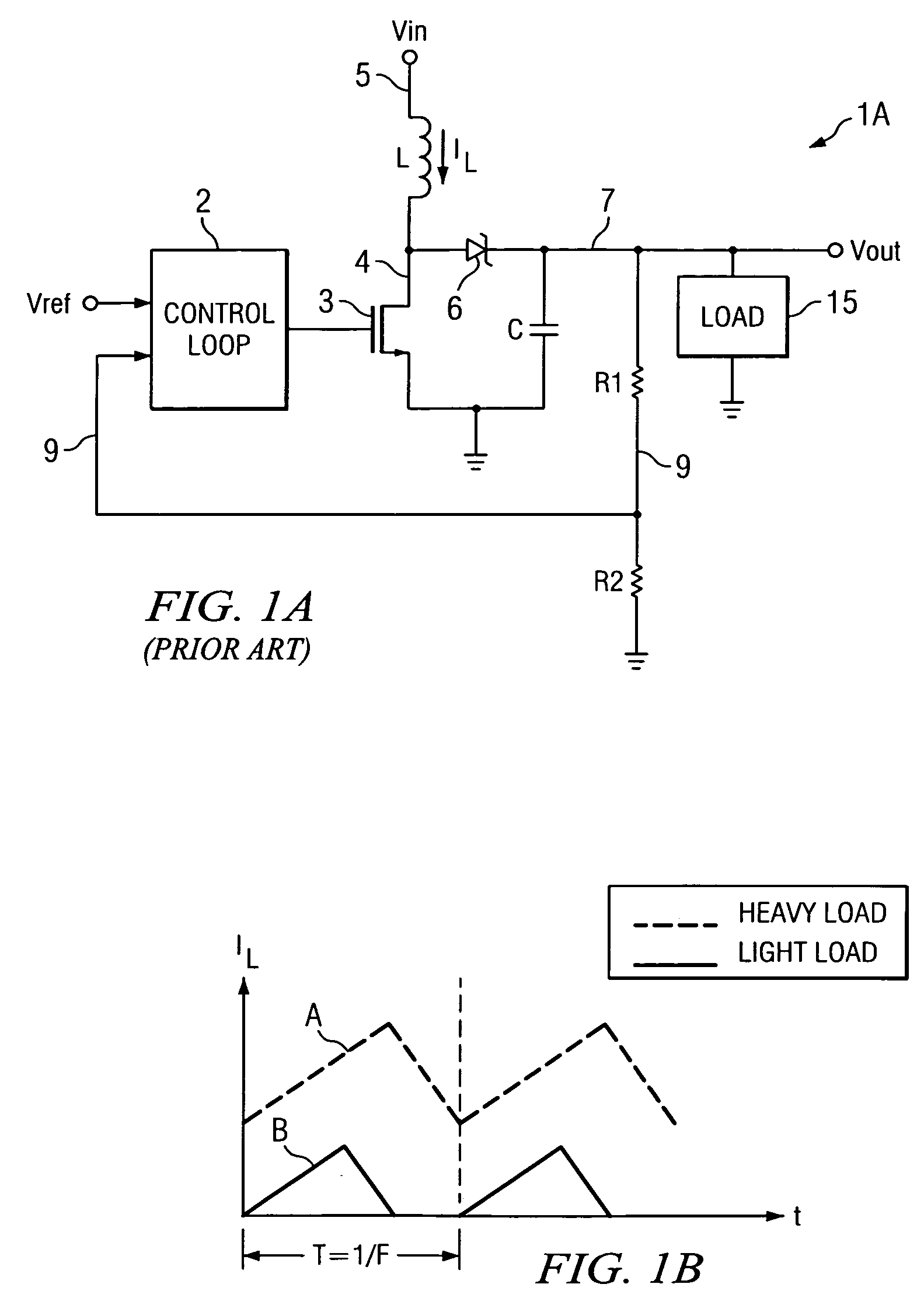
However, since efficiency is at the core of DC-to-DC boost converter design, the circuit structure shown in FIG. 1A is not well-suited for low voltage designs because the typical several hundred millivolt voltage drop across diode 6 tends to substantially diminish the overall efficiency, especially in applications in which Vin and Vout both have very low values.
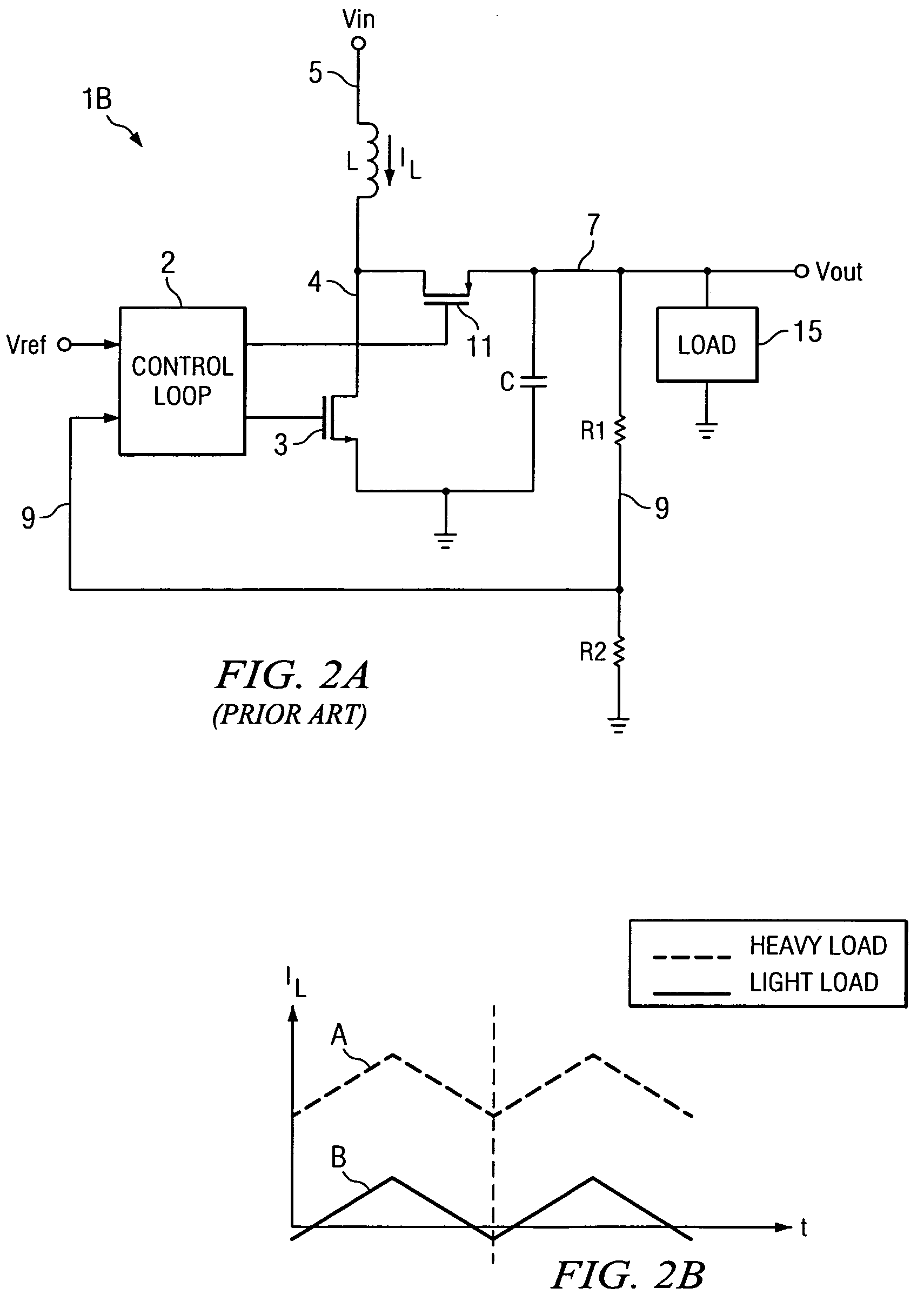
This is undesirable since it increases the power loss in the boost converter and also because the input voltage source circuit (not shown) which supplies Vin may not be able to handle such “backflow” current.
However, the foregoing technique requires that comparator 12 have a very small input offset voltage and a very fast response time.
If comparator 12 has a positive offset voltage, that means inductor current IL has to build up to a relatively large negative value to trigger comparator 12, causing it to switch too late, which is undesirable because from the standpoint of power efficiency.
In the opposite case, if comparator 12 has a large negative input offset voltage, comparator 12 will be prematurely triggered and change state too soon, which also results in undesired power loss.
However, implementation of such a comparator is generally costly because fast response time or low delay usually necessitates use of circuit implementations that require increased power consumption, and because achieving low input offset voltages often necessitates use of complex, expensive circuit techniques, such as auto-zeroing circuitry.

Method used


Image

  • Predictive duty ratio generating circuit and method for synchronous boost converters operating in PFM mode
  • Predictive duty ratio generating circuit and method for synchronous boost converters operating in PFM mode
  • Predictive duty ratio generating circuit and method for synchronous boost converters operating in PFM mode

Examples


Embodiment Construction

[0035]Referring to FIG. 4A, synchronous DC-to-DC boost converter 10 (referred to as “boost converter 10”) includes a predictive duty cycle controller 2 which receives Vin as an input voltage, Vref as a reference voltage, a feedback control signal VFB on conductor 9, and either an internal or external clock signal. An output VGN of predictive duty cycle controller 2 is coupled by conductor 8A to the gate of N-channel output power transistor 3, the source of which is connected to ground. The drain of transistor 3 is connected by conductor 4 to one terminal of an external (off-chip) inductor L (which, for example, may have and inductance value from 1 to 10 μH), the other terminal of which is connected by conductor 5 to an input circuit or device (not shown) that produces the input voltage Vin. A current IL flows through inductor L. Conductor 4 is also connected to the drain of P-channel output power transistor 4, the source of which is connected by conductor 7 to provide the output vol...


PUM


Abstract

A synchronous DC-to-DC converter includes an inductor coupled to receive an input voltage, a first transistor having a source coupled to a first reference voltage and a drain coupled to the inductor, and a second transistor having a source coupled to an output conductor to produce an output voltage and a drain coupled to the inductor. A feedback signal representative of a value of the output voltage is generated, and a switch control signal is produced in response to the input voltage and a second reference voltage. The second transistor is turned off in response to the switch control signal each time the inductor current has decayed to zero to prevent reverse current flow through the inductor. A regulating signal indicates whether or not the feedback voltage exceeds the second reference voltage, to regulate the output voltage in a pulse-frequency modulation mode.

Description

BACKGROUND OF THE INVENTION[0001]The present invention relates generally to synchronous DC-to-DC boost converters operating in pulse-frequency modulation (PFM) mode, and more particularly to implementations including improvements which avoid undesired transfer of charge back into an input signal source when the direction of the inductor current reverses, and which also avoid the need for use of a costly, high-speed, high precision comparator to accomplish suitably fast, accurate operation.[0002]FIG. 1A shows a basic prior art DC-to-DC boost converter 1A. In a synchronous DC-to-DC boost converter the output voltage Vout is generally greater than the input voltage Vin. In boost converter 1A, N-channel power switch transistor 3 is turned on to build up the current IL flowing through an inductor L to a conductor 4 which is connected to the drain of power switch transistor 3 and also to the anode of a rectifier diode switch 6. The rising slopes of inductor current IL in FIG, 1B show this...

Claims


Application Information

Patent Timeline
IPC IPC(8): H02M3/335
CPCH02M3/156Y02B70/1466H02M2001/0022H02M3/1588H02M1/0022Y02B70/10
Inventor WANG, BINAN
Owner TEXAS INSTR INC
Learn More