Semiconductor optoelectronic device and method of fabricating the same

a semiconductor optoelectronic and optoelectronic technology, applied in the direction of instruments, semiconductor lasers, optical elements, etc., can solve the problems of difficult to improve the internal quantum efficiency and optical power of a semiconductor optoelectronic device, the composition ratio and the thickness of al of alsub>x/sub>ga/sub>1x/sub>n are limited, and the internal loss is reduced. , to achieve the effect of improving internal quantum

Active Publication Date: 2008-04-24
SAMSUNG ELECTRONICS CO LTD
View PDF5 Cites 262 Cited by
  • Summary
  • Abstract
  • Description
  • Claims
  • Application Information

AI Technical Summary

Benefits of technology

[0008]Example embodiments provide a semiconductor opto-electronic device that may be capable of increasing the optical confinement factor (OCF) and reducing internal loss to improve internal quantum efficiency and reliability. In addition, the semiconductor opto-electronic device may have higher efficiency and may be capable of increasing the optical gain to reduce the threshold current of a laser so as to reduce the operation input power.

Problems solved by technology

Thus, cracks are formed.
As a result, the composition ratio and the thickness of Al of AlxGa1−xN are limited.
Thus, it is difficult to improve the internal quantum efficiency and optical power of a semiconductor opto-electronic device.

Method used


Image

  • Semiconductor optoelectronic device and method of fabricating the same
  • Semiconductor optoelectronic device and method of fabricating the same
  • Semiconductor optoelectronic device and method of fabricating the same

Examples


Embodiment Construction

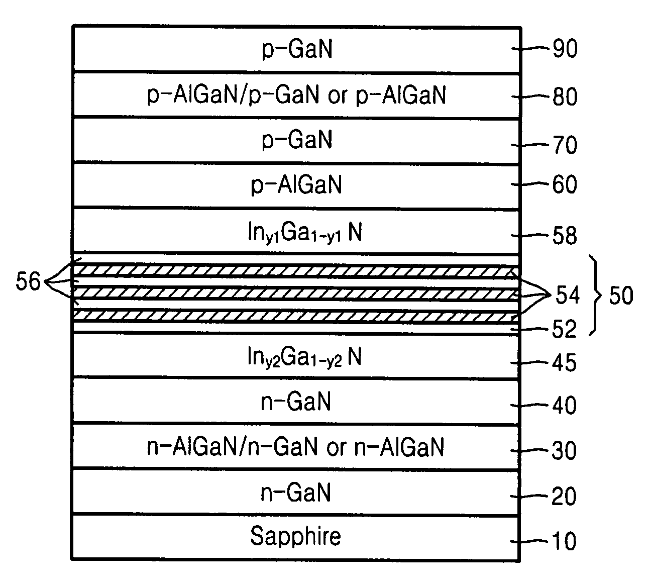
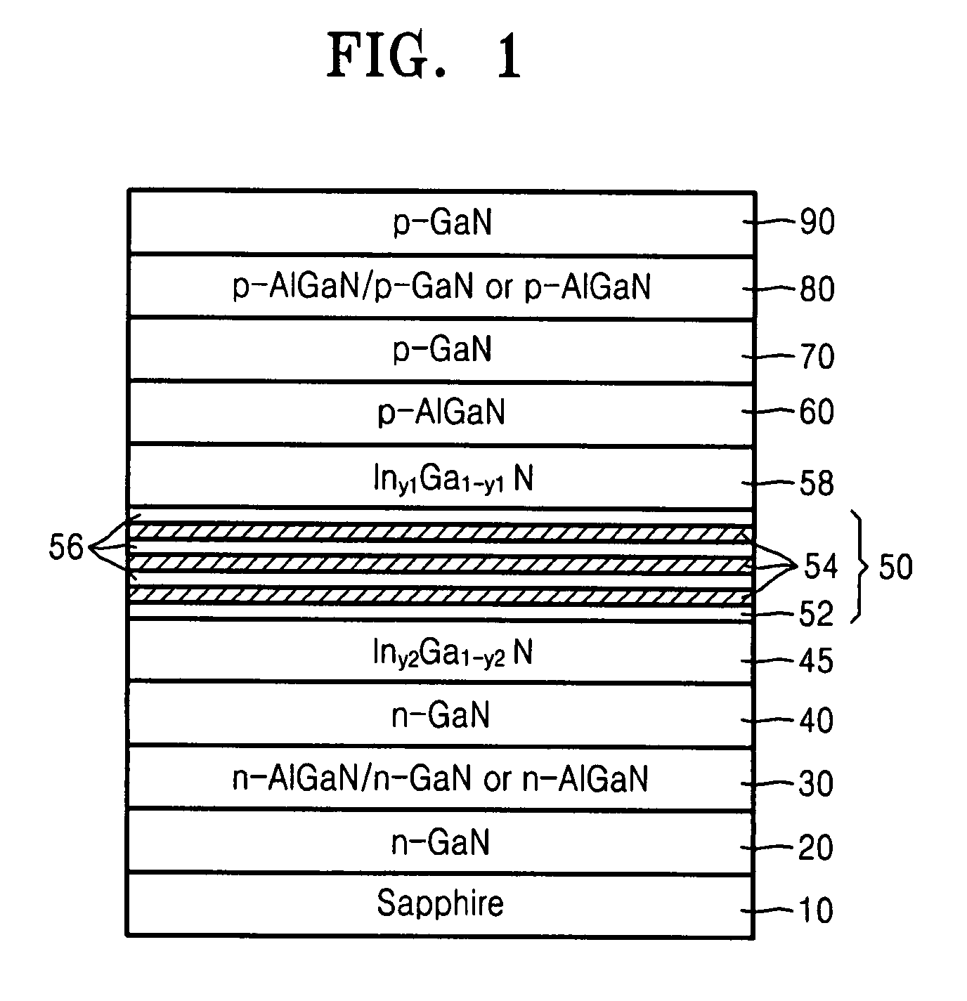
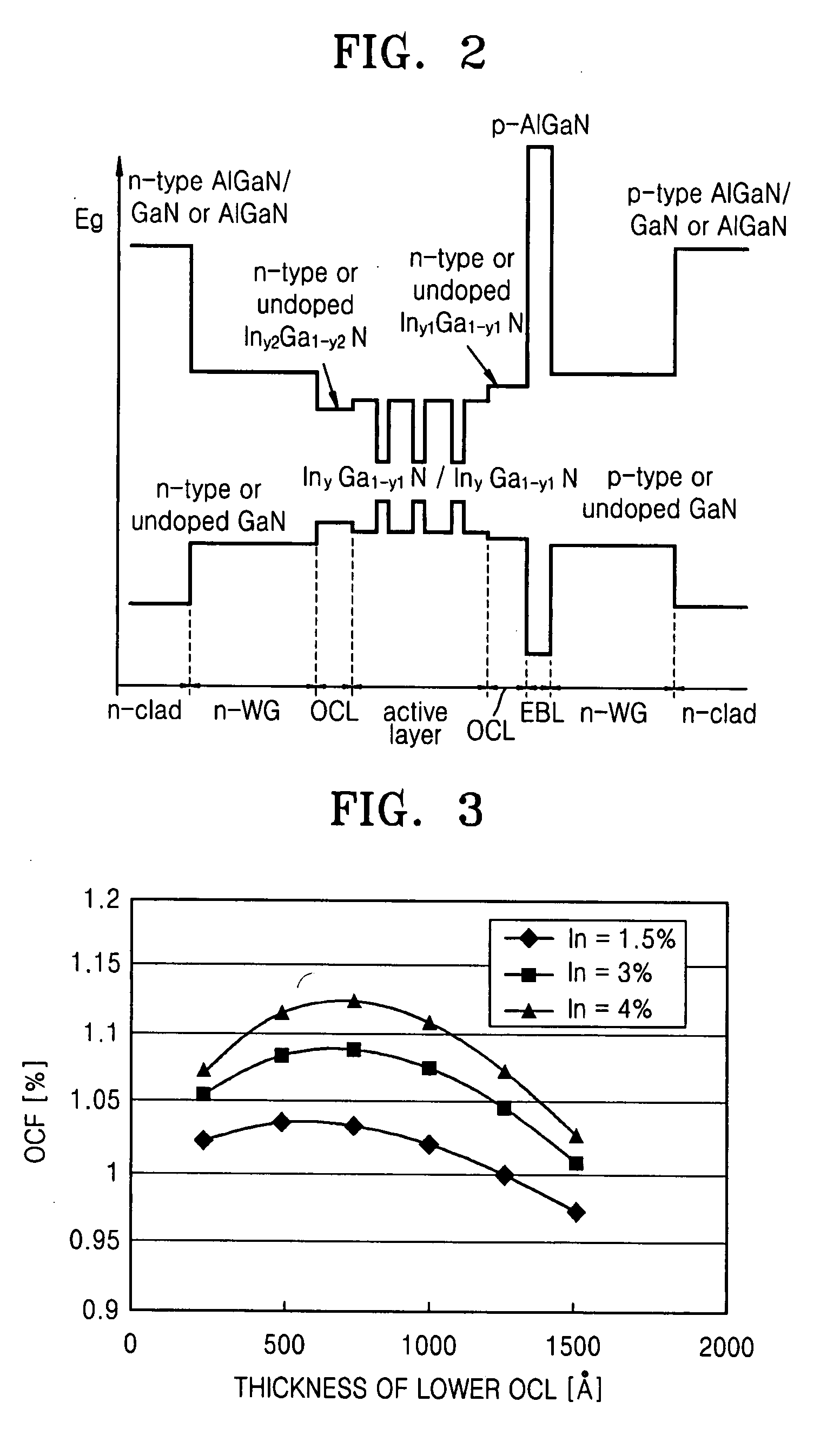
[0018]Reference will now be made in detail to example embodiments, examples of which are illustrated in the accompanying drawings. However, example embodiments are not limited to the embodiments illustrated hereinafter, and the embodiments herein are rather introduced to provide easy and complete understanding of the scope and spirit of example embodiments. In the drawings, the thicknesses of layers and regions are exaggerated for clarity.

[0019]It will be understood that when an element or layer is referred to as being “on,”“connected to” or “coupled to” another element or layer, it may be directly on, connected or coupled to the other element or layer or intervening elements or layers may be present. In contrast, when an element is referred to as being “directly on,”“directly connected to” or “directly coupled to” another element or layer, there are no intervening elements or layers present. Like reference numerals refer to like elements throughout. As used herein, the term “and / or...


PUM


Abstract

Provided is a semiconductor opto-electronic device that may comprise an active layer including a quantum well and a barrier layer on a substrate, upper and lower waveguide layers on and underneath the active layer, respectively, and upper and lower clad layers on and underneath the upper and lower waveguide layers, respectively. The semiconductor opto-electronic device may further comprise an upper optical confinement layer (OCL) between the active layer and the upper waveguide layer and having an energy gap smaller than the energy gap of the upper waveguide layer and equal to or larger than the energy gap of the barrier layer, and a lower OCL between the active layer and the lower waveguide layer and having an energy gap smaller than the energy gap of the lower waveguide layer and equal to or smaller than the energy gap of the barrier layer. Also provided is a method of fabricating the semiconductor opto-electronic device.

Description

PRIORITY STATEMENT[0001]This application claims priority under Korean Patent Application No. 2006-0101579, filed on Oct. 18, 2006, in the Korean Intellectual Property Office (KIPO), the entire contents of which are herein incorporated by reference.BACKGROUND[0002]1. Field[0003]Example embodiments relate to a semiconductor optoelectronic device having higher optical efficiency and method of fabricating the same.[0004]2. Description of the Related Art[0005]A semiconductor laser device is one kind of a nitride-based compound semiconductor opto-electronic device. Such nitride-based light emitting devices use sapphire as the material for forming the substrate. In general, a wave guide layer is formed of GaN to guide light formed in an active layer of the nitride-based laser diode. A clad layer is formed of AlxGa1−xN to confine light and electrons.[0006]AlxGa1−xN has a larger energy gap than GaN and a larger refractive index difference from InGaN as an active layer than GaN as a waveguide...

Claims


Application Information

Patent Timeline
Patent Type & Authority Applications(United States)
IPC IPC(8): G02B6/12
CPCB82Y20/00H01L33/02H01L33/06H01L33/32H01S5/0014H01S5/34333H01S5/2009H01S5/321H01S5/3213H01S5/3403H01S5/3406H01S5/2004H01L31/02
Inventor SON, JOONG-KONRYU, HAN-YOULSAKONG, TANPAEK, HO-SUNLEE, SUNG-NAM
Owner SAMSUNG ELECTRONICS CO LTD
Why Eureka
Try Eureka