

Methods and devices employing metal layers in gates to introduce channel strain
a metal layer and gate technology, applied in the field of semiconductor devices, can solve the problems of reducing the effectiveness of stress inducing layers and significant impact on power consumption and switching performance, and achieve the effects of facilitating stress inducing layers, improving device performance, and facilitating channel mobility
- Summary
- Abstract
- Description
- Claims
- Application Information
AI Technical Summary
Benefits of technology
Problems solved by technology
Method used
Image

Examples
Embodiment Construction
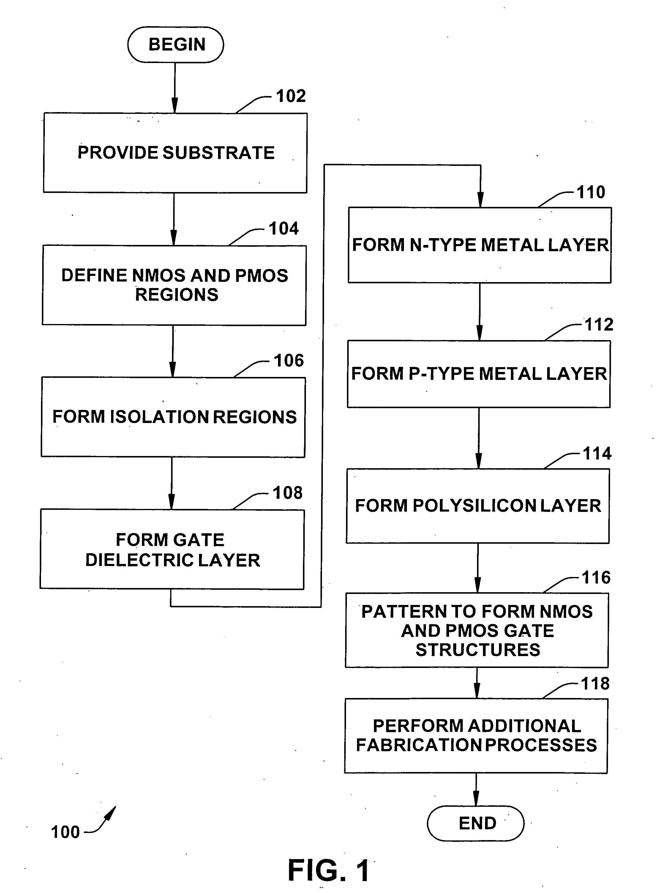
[0016]One or more implementations of the present invention will now be described with reference to the attached drawings, wherein like reference numerals are used to refer to like elements throughout, and wherein the illustrated structures are not necessarily drawn to scale.
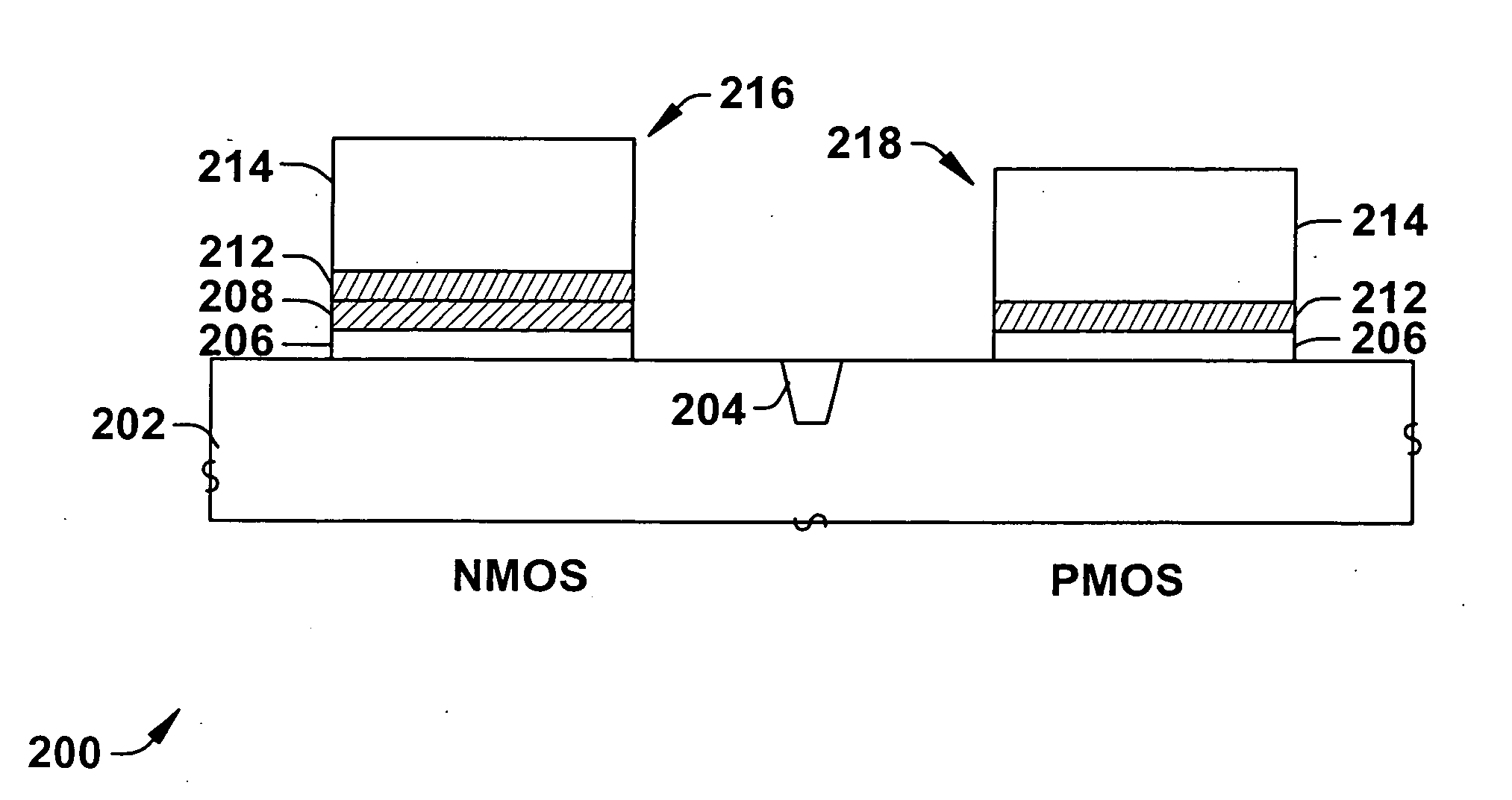
[0017]The various aspects of the invention employ one or more stress inducing metal gate layers to facilitate channel mobility for transistor devices. The metal gate layers are part of gate structures and can be individually tailored to induce tensile strain for NMOS devices and compress strain for PMOS devices. By facilitating channel mobility, other device performance characteristics can be improved such as, improved switching speed and low-power and the like.
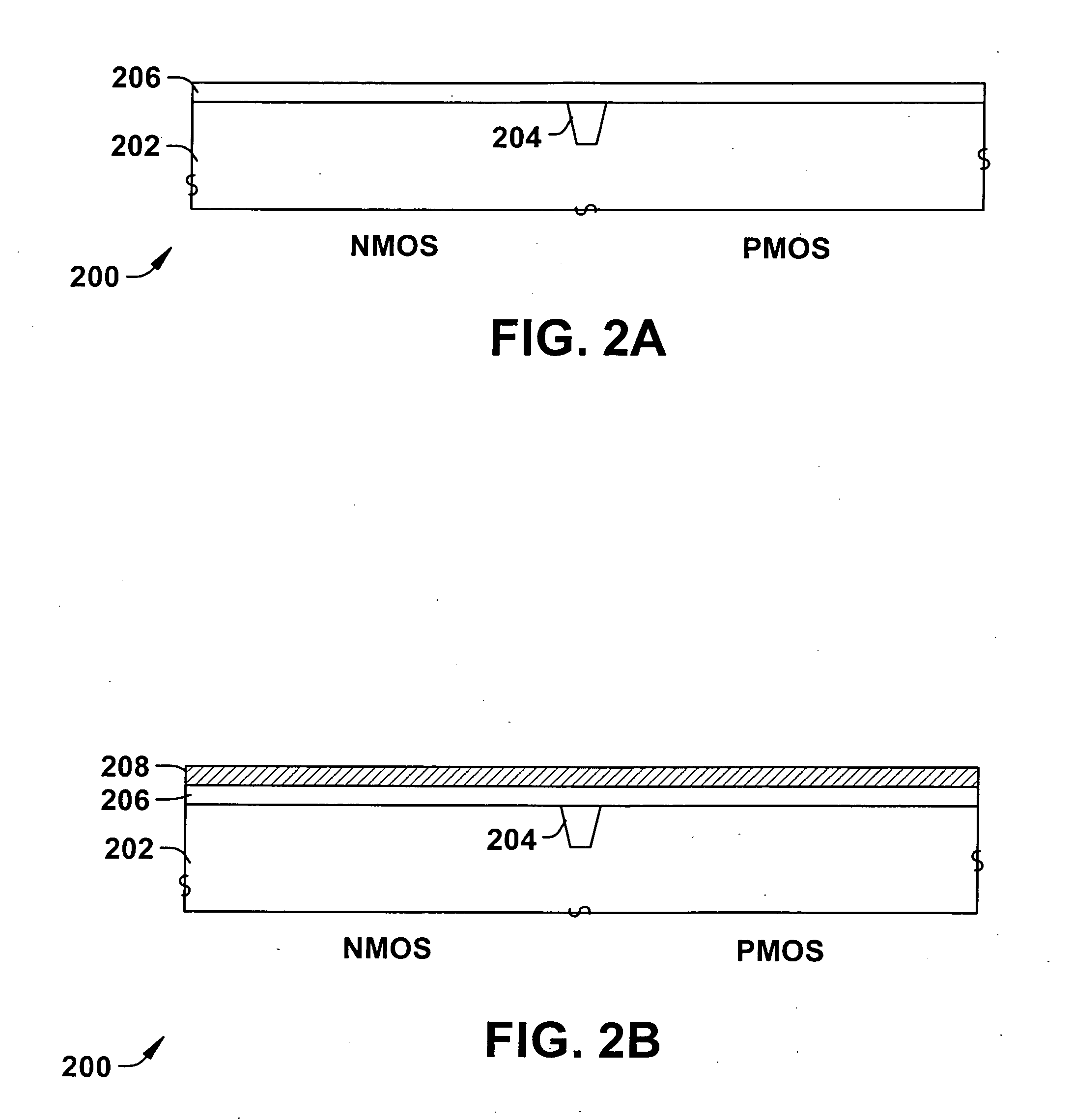
[0018]The inventors of the present invention note that pre-metal deposition (PMD) liners can be employed to induce strain into channel regions of transistor devices and, thereby, facilitate channel mobility. PMD liners are formed over gate structures and a...
PUM
| Property | Measurement | Unit |
|---|---|---|
| temperature | aaaaa | aaaaa |
| thickness | aaaaa | aaaaa |
| temperature | aaaaa | aaaaa |
Abstract
Description
Claims
Application Information