Non-volatile resistance switching memories and methods of making same

Active Publication Date: 2008-05-08
SYMETRIX MEMORY
View PDF11 Cites 275 Cited by
  • Summary
  • Abstract
  • Description
  • Claims
  • Application Information

AI Technical Summary

Benefits of technology

[0011]The invention provides an integrated circuit memory having a memory cell including: a semiconductor having a first active area, a second active area, and a channel between the active areas; and a layer of a variable resistance material (VRM) directly above the channel. Preferably, the variable resistance material comprises a correlated electron material (CEM). Preferably, the memory cell further includes a first conductive layer between the VRM and the channel. Preferably, the integrated circuit further includes a second conductive layer directly above the VRM layer. Preferably, the first conductive layer directly contacts the channel. Preferably, the first conductive layer comprises a plurality of conductive layers. Preferably, the memory cell may further include a layer of an insulating material between the VRM and the channel. Preferably, the memory cell comprises a field effect transistor (FET), such as a JFET structure or a MESFET structure, or the memory cell may comprise a MOSFET structure.
[0012]In anot

Problems solved by technology

Once these devices left the factory, they could not be re-written.
However, the worse limiting factor is the limited number of erase/write cycles to no more than slightly over 600,000—or of the order of 105-106.
FeRAMs (Ferroelectric RAMs) provide low power, high write/read speed, and endurance for read/write cycles exceeding 10 billion times. Magnetic memories (MRAMs) provide high write/read

Method used


Image

  • Non-volatile resistance switching memories and methods of making same
  • Non-volatile resistance switching memories and methods of making same
  • Non-volatile resistance switching memories and methods of making same

Examples


Embodiment Construction

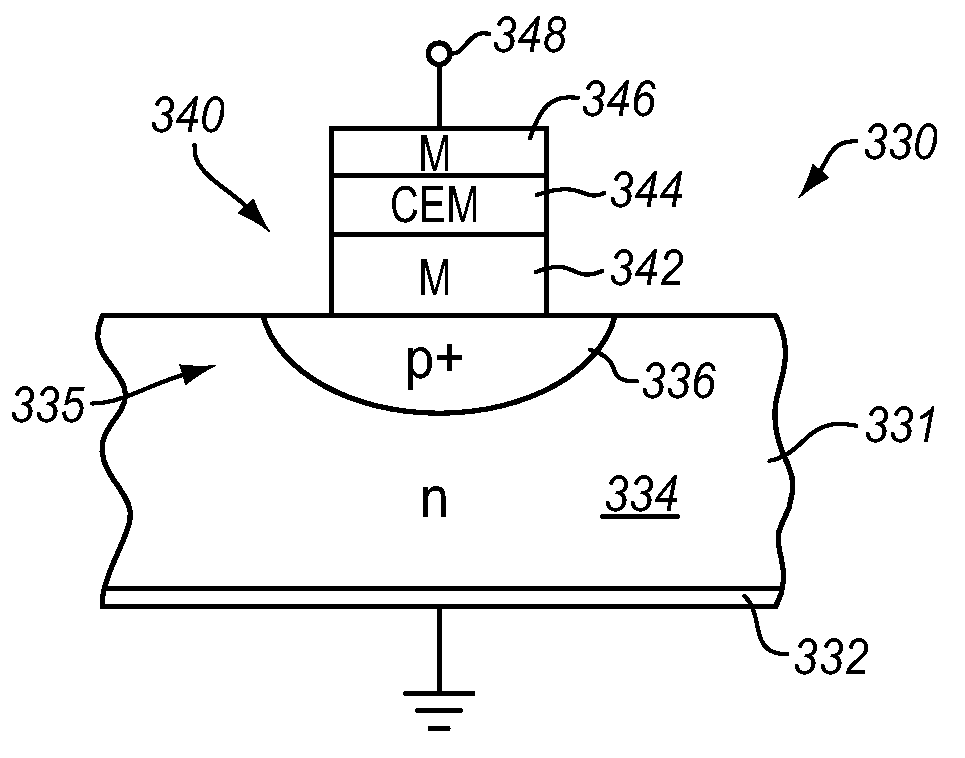
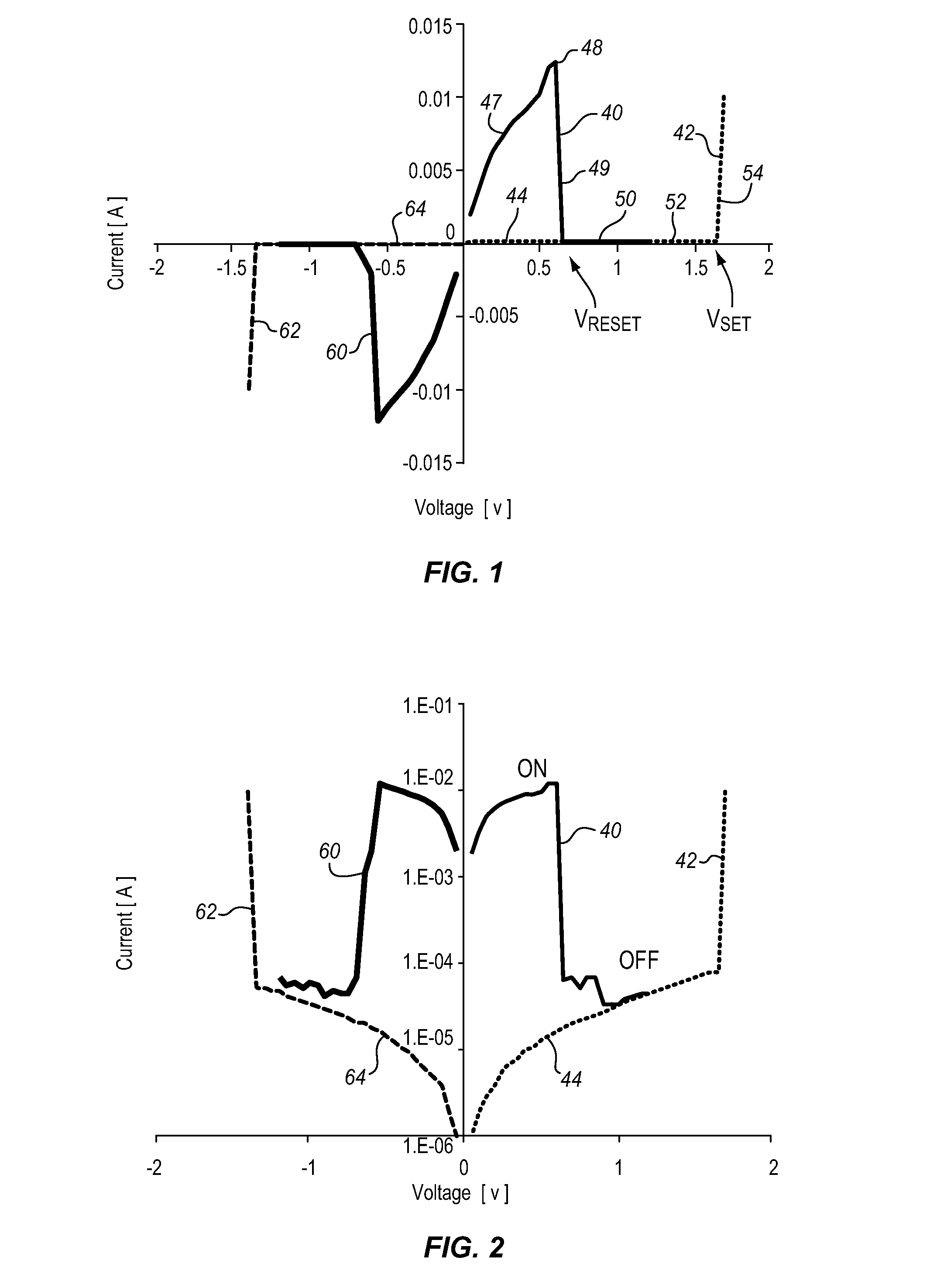
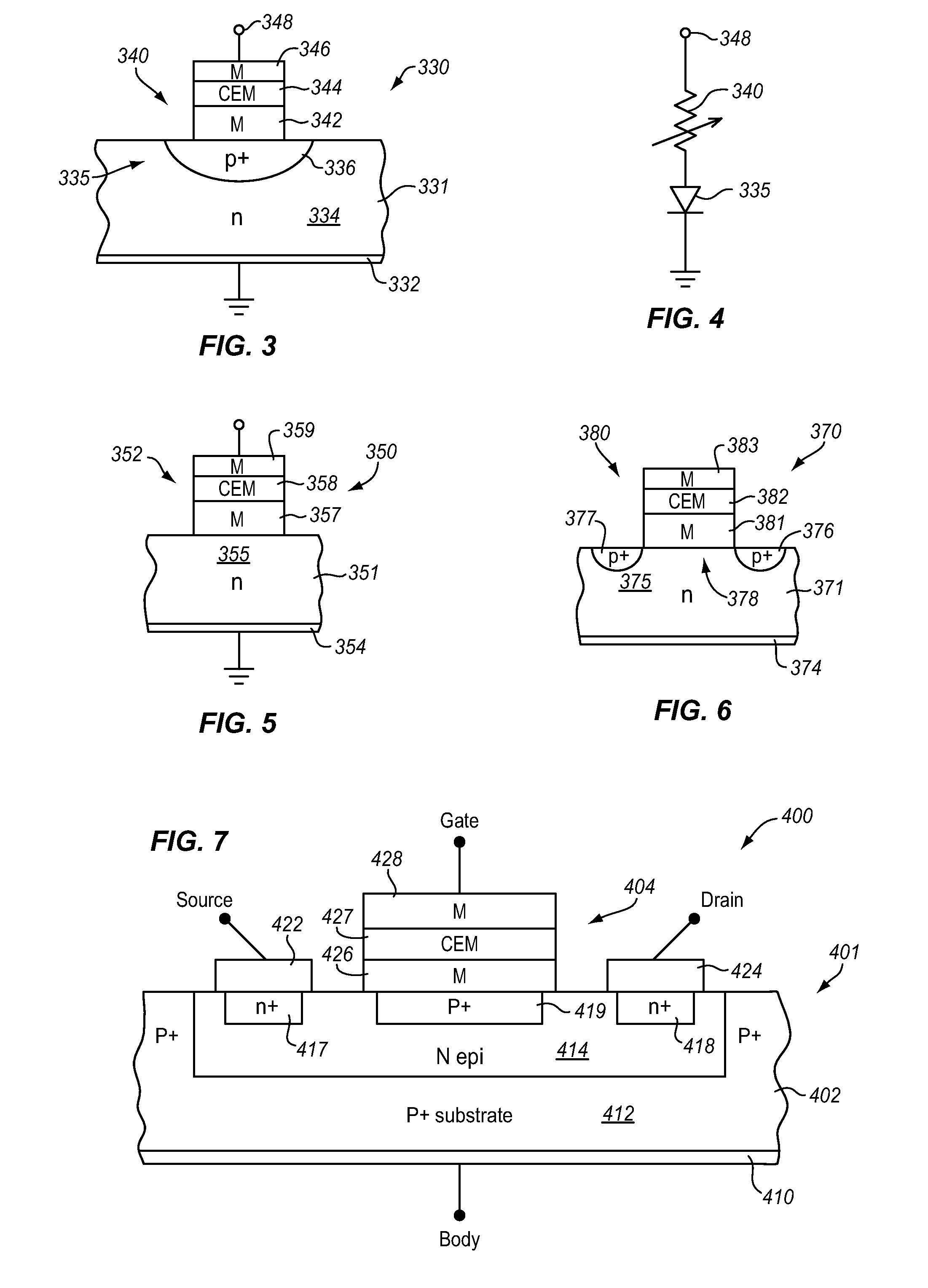
[0046]The present disclosure relates to novel memory architectures for variable resistance materials. In this disclosure, a variable resistance material may be referred to as a VRM. In the exemplary discussion required by the patent law, the disclosure focuses on transition metal oxide variable resistance materials, though the invention is applicable to other variable resistance materials as well. Nickel oxide, NiO, is disclosed as the exemplary transition metal oxide. The samples of NiO materials discussed herein are doped with extrinsic ligands which stabilize the variable resistance properties, though this is not a requirement to be a variable resistance material. All of the exemplary NiO variable resistance materials disclosed herein also include at least a carbon ligand, which may indicated by NiO(Cx). This also is not a requirement for a variable resistance material, but is simply exemplary.

[0047]The exemplary variable resistance materials discussed herein are Correlated Elect...


PUM


Abstract

An integrated circuit memory cell including: a semiconductor having a first active area, a second active area, and a channel between the active areas; and a layer of a variable resistance material (VRM) directly above the channel. In one embodiment, there is a first conductive layer between the VRM and the channel and a second conductive layer directly above the VRM layer. The VRM preferably is a correlated electron material (CEM). The memory cell comprises a FET, such as a JFET or a MESFET. In another embodiment, there is a layer of an insulating material between the VRM and the channel. In this case, the memory cell may include a MOSFET structure.

Description

CROSS-REFERENCE TO RELATED APPLICATIONS[0001]This application is a Non-Provisional Application claiming the benefit of: Provisional (35 USC 119(e)) Application No. 60 / 858,218 filed on Nov. 8, 2006; Provisional (35 USC 119(e)) Application No. 60 / 904,768 filed on Mar. 2, 2007; Provisional (35 USC 119(e)) Application No. 60 / 906,158 filed on Mar. 9, 2007; and Provisional (35 USC 119(e)) Application No. 60 / 913,245 filed on May 21, 2007. All of the foregoing provisional applications are hereby incorporated by reference to the same extent as though fully disclosed herein.FIELD OF THE INVENTION[0002]The invention in general relates to integrated circuit memories, and in particular, to the formation of non-volatile integrated circuit memories containing materials which exhibit a change in resistance.BACKGROUND OF THE INVENTION[0003]Non-volatile memories are a class of integrated circuits in which the memory cell or element does not loose its state after the power supplied to the device is tu...

Claims


Application Information

Patent Timeline
IPC IPC(8): G11C11/00H01L21/00
CPCG11C2213/32H01L45/1233G11C2213/72G11C2213/75G11C2213/79H01L27/2409H01L27/2436H01L29/685H01L45/04H01L45/1226H01L45/146B82Y10/00G11C13/0007G11C13/003G11C11/24G11C2213/53H10B63/20H10B63/30H10N70/20H10N70/823H10N70/826H10N70/8833
Inventor BRUBAKER, MATTHEW D.PAZ DE ARAUJO, CARLOS A.CELINSKA, JOLANTA
Owner SYMETRIX MEMORY
Why Eureka
Try Eureka