Cleaning solutions and methods of cleaning boards using the same

a technology of cleaning solution and cleaning solution, which is applied in the preparation of detergent mixture composition, cleaning using liquids, detergent compounding agents, etc., can solve the problems of defect (, crack) that form between the ni/au coating layer and the solder ball, and the impact resistance of the semiconductor device package can deteriorate remarkably, so as to achieve effective cleaning

Inactive Publication Date: 2008-05-15
SAMSUNG ELECTRONICS CO LTD
View PDF8 Cites 11 Cited by
  • Summary
  • Abstract
  • Description
  • Claims
  • Application Information

AI Technical Summary

Benefits of technology

[0014]In one aspect, the present invention provides a cleaning solution suitable for effectively cleaning an organic solderability preservative (OSP) from the surface of a board.
[0015]In another aspect, the present invention also provides a method of cleaning a board that can effectively clean an OSP from the surface of a board.

Problems solved by technology

However, when the lead-free solder ball is used in a semiconductor device package, the impact resistance of the semiconductor device package can deteriorate remarkably.
In particular, this impact resistance can be significant when the semiconductor device package is mounted on an electronic equipment, such as a mobile phone or the like, that is easily exposed to impact.
The intermetallic compound containing the gold generated by combining the Ni / Au coating layer and the solder ball pad may cause a defect (e.g., a crack) to form between the Ni / Au coating layer and the solder ball due to the inherent brittleness of gold.
This crack may cause the solder ball to become easily separated from the solder ball pad when a physical impact is applied.
However, the OSP can become thermally transformed due to its poor heat resistance during the fabrication of the semiconductor device package, and the solder ball pad may still be oxidized.
The thermal transformation of the OSP and the oxidization of the solder ball pad may cause a wetting defect in a subsequent process of attaching the solder ball.
When the thermally transformed OSP, which remains on the surface of the solder ball pad, is not completely removed through the cleaning process, the remaining thermally transformed OSP may have an adverse effect on the subsequent process of attaching the solder ball.
When the OSP formed on the surface of the solder ball pad is removed using the above-described method of cleaning the PCB, it can take a long time (e.g., at least 5 minutes) to remove the OSP.
In addition, depending on the amount of the dotting flux and how accurately it is positioned, quality deviation may occur in removing the OSP.
This deviation can degrade solder joint reliability (SJR).
Furthermore, the overall process can be complicated because the degree of OSP removal from the solder ball pad is inspected to prevent degradation of the SJR during the subsequent process of attaching the solder ball.

Method used


Image

  • Cleaning solutions and methods of cleaning boards using the same

Examples


Embodiment Construction

[0030]Preferred embodiments of the present invention will be described below in more detail with reference to accompanying drawings. The present invention may, however, be embodied in different forms and should not be constructed as limited to the embodiments set forth herein. Rather, these embodiments are provided such that this disclosure will be thorough and complete, and will fully convey the scope of the present invention to those skilled in the art. Therefore, shapes of elements are exaggerated for clarity of illustration in the drawings. Since preferred embodiments are provided below, the order of the reference numerals given in the description is not limited thereto. In the drawings, like reference numerals refer to like elements throughout.

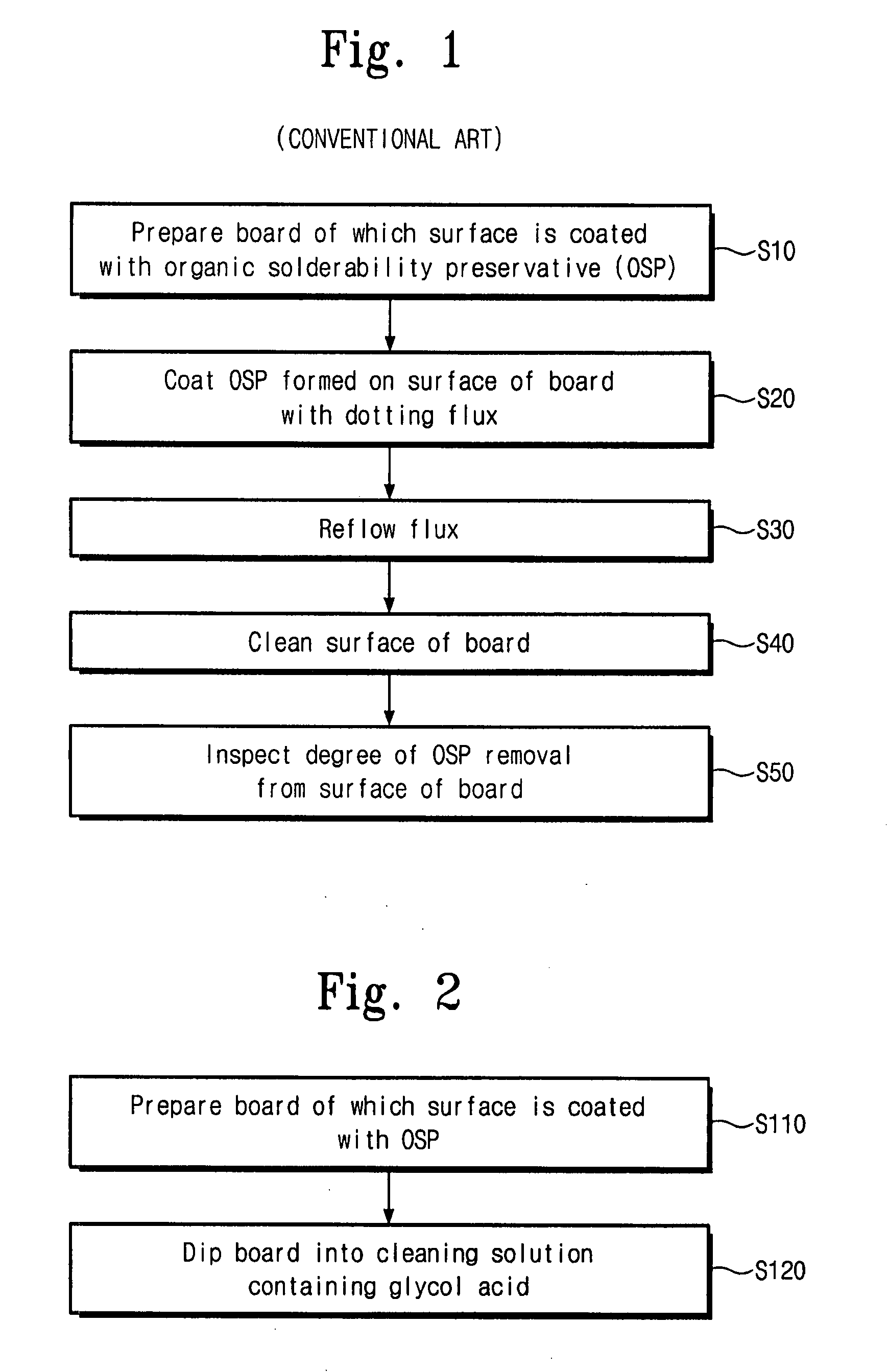
[0031]Table 1 illustrates results of a bending test for a printed circuit board (PCB) mounted on a system board.

[0032]Referring to table 1, solder ball pads of the printed circuit board and the system board are finished in three ways. Fir...


PUM


Abstract

A method of cleaning a board includes dipping a board having a surface on which an organic solderability preservative (OSP) is provided into a cleaning solution having glycolic acid, a surfactant and water.

Description

CROSS-REFERENCE TO RELATED APPLICATIONS[0001]This U.S. non-provisional patent application claims priority under 35 U.S.C. § 119 to Korean Patent Application No. 10-2006-112975, filed on Nov. 15, 2006, the entire contents of which are hereby incorporated by reference.FIELD OF THE INVENTION[0002]The present invention disclosed herein relates to cleaning solutions and methods of cleaning a board using the same, such as, for example cleaning solutions for cleaning organic solderability preservative (OSP) from a board surface.BACKGROUND[0003]To date, semiconductor device packages have been continuously developed with emphasis on miniaturization, reduction of inductance to make them more compatible with high-speed semiconductor chips, and reduction of fabrication cost.[0004]Semiconductor packages are designed such that an increasing number of external connection terminals can be provided within a limited area. To this end, the external connection terminal of the semiconductor device packa...

Claims


Application Information

Patent Timeline
Patent Type & Authority Applications(United States)
IPC IPC(8): B08B3/04
CPCC11D3/2068C11D3/2086H05K2203/122H05K3/26H05K3/282C11D11/0047H01L21/302
Inventor JUNG, KY-HYUNSIN, WHA-SUKIM, SANG-JUNKIM, JUNG-HYEONCHOI, WON-SEOK
Owner SAMSUNG ELECTRONICS CO LTD
Why Eureka
Try Eureka