Semiconductor Wafer Fabricating Method and Semiconductor Wafer Mirror Edge Polishing Method

a semiconductor and fabricating method technology, applied in the direction of edge grinding machines, manufacturing tools, lapping machines, etc., can solve the problems of degrading a roll-off amount, affecting the yield, and unable to completely avoid defects, etc., to achieve the effect of excessive polishing and low cos

Inactive Publication Date: 2008-05-15
SHIN-ETSU HANDOTAI CO LTD
View PDF2 Cites 26 Cited by
  • Summary
  • Abstract
  • Description
  • Claims
  • Application Information

AI Technical Summary

Benefits of technology

[0031]As a result, a scratch or an impression on an edge surface of the chamfered part after double-side polishing can be removed at a low cost, excessive polishing caused when the polishing p

Problems solved by technology

Accordingly, a scratch or an impression is formed on an edge surface of the wafer chamfered part, and such a defect cannot be completely avoided even if a resin softer than silicon is used for a carrier inner peripheral surface.
At a film forming step or a resist resin film applying step in device fabrication, an oxide film or a nitride film is formed at a chamfered part or a resist film adheres to the chamfered part in some cases but, if a scratch or an impression is present at the chamfered part, such film components cannot be removed at a subsequent cleaning step and others and remains as a particle generation source, which becom

Method used


Image

  • Semiconductor Wafer Fabricating Method and Semiconductor Wafer Mirror Edge Polishing Method
  • Semiconductor Wafer Fabricating Method and Semiconductor Wafer Mirror Edge Polishing Method
  • Semiconductor Wafer Fabricating Method and Semiconductor Wafer Mirror Edge Polishing Method

Examples


example

[0089]Such a double-side polishing apparatus as depicted in FIG. 6 was used to perform double-side polishing with respect to a silicon wafer having a diameter of 300 mm obtained by sequentially effecting respective processes, i.e., slicing, chamfering, lapping, and etching.

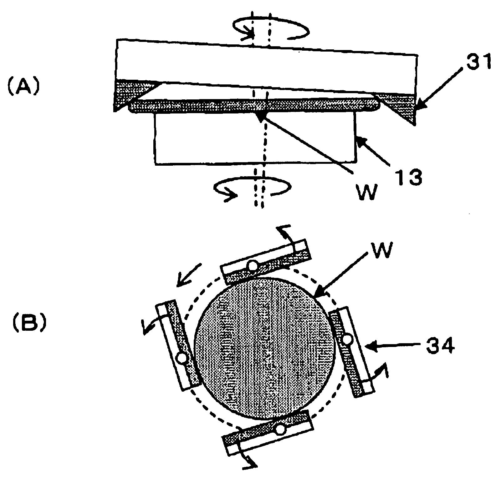
[0090]After double-side polishing, an acrylic resin (a product name: Sky Coat manufactured by Nikka Seiko Co., Ltd.) was applied by using a spin coater to form protection films each having a thickness of approximately 3 μm on both surfaces of the wafer W. At this time, the number of revolutions of the spin coater was determined as 1200 rpm, the protection films were formed on the main surfaces alone of the front and back surfaces, and the protection film was prevented from being formed on a wafer edge surface. Then, a chamfered surface on each main surface side at a chamfered part of the wafer W was brought into contact with a polishing pad to mirror-polish the chamfered part (FIG. 2(A): the protection film is sho...


PUM


Abstract

There is provided a semiconductor wafer fabricating method comprising at least: a double-side polishing step of mirror-polishing a front surface and a back surface of a semiconductor wafer; and a mirror edge polishing step of mirror-polishing a chamfered part of the double-side-polished semiconductor wafer, wherein a protection film made of a resin which suppresses polishing is formed on the front surface or both the front and back surfaces of the semiconductor wafer after the double-side polishing step, then the mirror edge polishing step is carried out, and thereafter the protection film made of a resin is removed. As a result, it is possible to provide a step of eliminating an increase in a cost due to, e.g., a facility investment or an increase in the number of steps as much as possible, removing a scratch or an impression on an edge surface of the chamfered part of the semiconductor wafer, and suppressing excessive polishing caused when a polishing pad enters a main surface of the wafer at the mirror edge polishing step of mirror-polishing the chamfered part of the wafer, thereby preventing a wafer outer peripheral shape, especially an edge roll-off from being degraded.

Description

TECHNICAL FIELD[0001]The present invention relates to a semiconductor wafer fabricating method, and more particularly to a semiconductor wafer fabricating method and a semiconductor wafer mirror edge polishing method capable of achieving a high flatness degree even at a wafer outer peripheral part when performing fabrication through, e.g., a double-side polishing step.BACKGROUND ART[0002]A semiconductor wafer used in fabrication of a semiconductor device is fabricated through each step, e.g., chamfering (grinding), lapping, etching, single-side polishing, or chamfered part polishing (mirror edge polishing) after slicing a silicon single crystal ingot grown by, e.g., a Czochralski method to be machined into a wafer shape.[0003]In recent years, with a reduction in design rules involved by high integration of a semiconductor device, a flatness degree required for a silicon wafer is becoming rigorous. Further, obtaining as many devices as possible from one wafer is desired, and a shape ...

Claims


Application Information

Patent Timeline
IPC IPC(8): H01L21/306
CPCB24B9/065H01L21/02021H01L21/02008B24B37/08H01L21/304
Inventor KATO, TADAHIROKUDO, HIDEO
Owner SHIN-ETSU HANDOTAI CO LTD
Why Eureka
Try Eureka