Epitaxially coated semiconductor wafer and device and method for producing an epitaxially coated semiconductor wafer

a technology of epitaxial coating and semiconductor wafer, which is applied in the direction of polycrystalline material growth, crystal growth process, transportation and packaging, etc., can solve the problem of increasing the occurrence of undesired crystal defects, dislocations and slippages, and undesired radial variation in the resistivity of the epitaxial layer, so as to avoid undesired crystal defects, good edge roll-off value, and good local planarity

Active Publication Date: 2008-05-22
SILTRONIC AG
View PDF7 Cites 28 Cited by
  • Summary
  • Abstract
  • Description
  • Claims
  • Application Information

AI Technical Summary

Benefits of technology

[0015]It was therefore an object of the invention to provide stress-free epitaxially coated semiconductor wafers having good edge roll-off values as well as good local planarity, while avoiding undesired crystal de

Problems solved by technology

They are then incorporated into the epitaxial layer, predominantly in the edge region of the front side of the semiconductor wafer, and therefore cause a more or less pronounced undesired radial variation in the resistivity of the epitaxial layer.
Another problem in the epitaxial coating of semiconductor wafers involves stresses in the epitaxially coated semiconductor wafers, which can lead to dislocations and slips.
Lower coating temperatures, however, lead to an increased occurrence of undesired crystal defects such as stacking faults or typical epitaxial defects which are known by the terms “hillocks”, “mounds” or “pits”.
Another disadvant

Method used


Image

  • Epitaxially coated semiconductor wafer and device and method for producing an epitaxially coated semiconductor wafer
  • Epitaxially coated semiconductor wafer and device and method for producing an epitaxially coated semiconductor wafer
  • Epitaxially coated semiconductor wafer and device and method for producing an epitaxially coated semiconductor wafer

Examples


Embodiment Construction

)

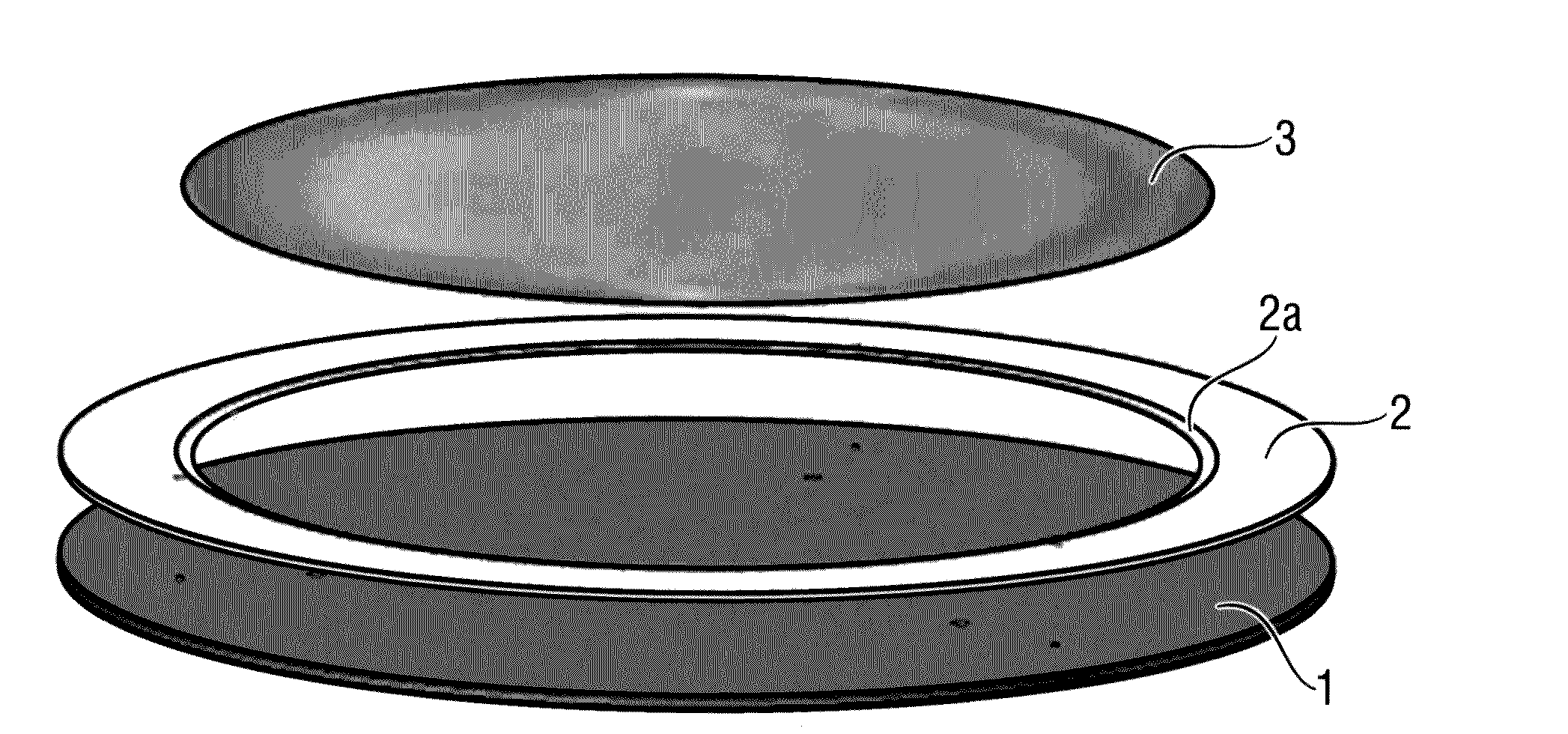
[0020]The invention thus relates to a device for supporting a semiconductor wafer during the deposition of a layer on a front side of the semiconductor wafer by chemical vapor deposition, for example in an epitaxial reactor, the reactor containing a susceptor which has a gas-permeable structure, and a ring placed on the susceptor which acts as a thermal buffer between the susceptor and the supported semiconductor wafer.

[0021]The susceptor is preferably one which has a porosity (pore volume / total volume) of at least 15% and a density of from 0.5 to 1.5 g / cm3. The necessary porosity and density of the susceptor may be obtained by suitable compression of fibers or particles during production of the susceptor. The susceptor preferably consists of graphite or graphite fibers, and is preferably coated with silicon carbide.

[0022]The device according to the invention comprises a ring which is placed on the susceptor, the ring preferably being selected in respect of its thickness and in res...


PUM

PropertyMeasurementUnit
Temperatureaaaaaaaaaa

Abstract

In a method for producing epitaxially coated semiconductor wafers, a multiplicity of prepared, front side-polished semiconductor wafers are successively coated individually with an epitaxial layer on their polished front sides at temperatures of 800-1200° C. in a reactor, while supporting the prepared semiconductor wafer over a susceptor having a gas-permeable structure, on a ring placed on the susceptor which acts as a thermal buffer between the susceptor and the supported semiconductor wafer, the semiconductor wafer resting on the ring, and its backside facing but not contacting the susceptor, so that gaseous substances are delivered from a region over the backside of the semiconductor wafer by gas diffusion through the susceptor into a region over the backside of the susceptor, the semiconductor wafer contacting the ring only in an edge region of its backside, wherein no stresses measurable by means of photoelastic stress measurement (“SIRD”) occur in the semiconductor wafer.

Description

BACKGROUND OF THE INVENTION[0001]1. Field of the Invention[0002]The invention relates to a semiconductor wafer having a front side coated by chemical vapor deposition (CVD) and to a method for producing this semiconductor wafer. The invention also relates to a device for supporting a semiconductor wafer during the deposition of a layer on a front side of the semiconductor wafer by chemical vapor deposition (CVD).[0003]2. Background Art[0004]During chemical vapor deposition, in particular the deposition of an epitaxial layer on a polished semiconductor wafer, two phenomena may occur, inter alia, which are known by the terms “autodoping” and “halo”.[0005]In “autodoping”, dopants pass from the backside of the semiconductor wafer via the gas phase into the deposition gas, which is fed over the front side of the semiconductor wafer. They are then incorporated into the epitaxial layer, predominantly in the edge region of the front side of the semiconductor wafer, and therefore cause a mor...

Claims


Application Information

Patent Timeline
IPC IPC(8): B32B3/00C23C16/458H01L21/36
CPCC23C16/4585C30B25/12H01L21/02381Y10T428/24612H01L21/02579H01L21/02634H01L21/02532H01L21/68735H01L21/20
Inventor SCHAUER, REINHARDWERNER, NORBERT
Owner SILTRONIC AG
Why Eureka
Try Eureka