Density-Based Layer Filler for Integrated Circuit Design

a density-based layer filler and integrated circuit technology, applied in the field of density-based layer filler for integrated circuit design and computer-aided design layout, can solve the problems of complex and time-consuming process of integrated circuit design, complex design process, and large number of dummy shapes added to a design, so as to reduce the risk of process yield and reduce the size of the layout databas

Active Publication Date: 2008-05-22
ORACLE INT CORP
View PDF4 Cites 83 Cited by
  • Summary
  • Abstract
  • Description
  • Claims
  • Application Information

AI Technical Summary

Benefits of technology

[0015]The density-based layer filler described herein may in some embodiments be integrated into the overall integrated circuit design flow, or may be implemented as a stand-alone tool to be executed outside of, or in parallel with, the standard design flow. The use of a density-based layer filler, as described herein, may in some embodiments reduce the risk of process yield problems, as compared to a flood filler, since the number of dummy shapes added to a design may be minimized. Use of a density-based layer filler may also substantially reduce the layout database size (when compared to the layout database produced by a flood filler) and may improve the runtime of analysis tools that depend on complete designs (i.e. with fill shapes inserted), such as extraction and noise analysis tools. The time to insert fill shapes may also be reduced, as only the necessary number of shapes is inserted. Thus, a density-based layer filling tool may execute faster than a comparable flood filler.

Problems solved by technology

Design of an electronic circuit, for example, an integrated circuit (IC), is a complicated and time-consuming process. FIG. 1 illustrates a typical design flow of an integrated circuit device from conception through the generation of a fabrication ready design layout.
The detailed design layout may require a very intensive and time-consuming design effort and is typically performed utilizing specialized computer aided design (CAD) or Electronic Design Automation (EDA) tools.
DRC may be a time-consuming, iterative process that often requires manual manipulation and interaction by the designer.
Deep sub-micron designs typically have stringent design rules that are often not recognized or not properly handled by existing EDA tools.
For example, a tool that is used to flood fill a given area of the design with metal on a particular metal layer (e.g., in order to attempt to meet a layer density rule) may introduce other errors.
Because EDA tools are increasingly relied upon to create design layouts, and because conventional EDA tools do not prevent the creation of certain violations, thousands of violations can be created that must be corrected.
Performing a DRC and manipulation of the design layout to correct these violations often requires manual interaction from the designer.
Creation of a violation-free design layout becomes a critical, time-consuming process.
Due to the complexity of the design and because the layout design flow can be repeated throughout the design process, manually fixing violations may not be an affordable approach.
For example, using a flood fill in some areas of the design may result in violations of a maximum density rule, or may introduce a violation of a complex spacing or overlap design rule.

Method used


Image

  • Density-Based Layer Filler for Integrated Circuit Design
  • Density-Based Layer Filler for Integrated Circuit Design
  • Density-Based Layer Filler for Integrated Circuit Design

Examples


Embodiment Construction

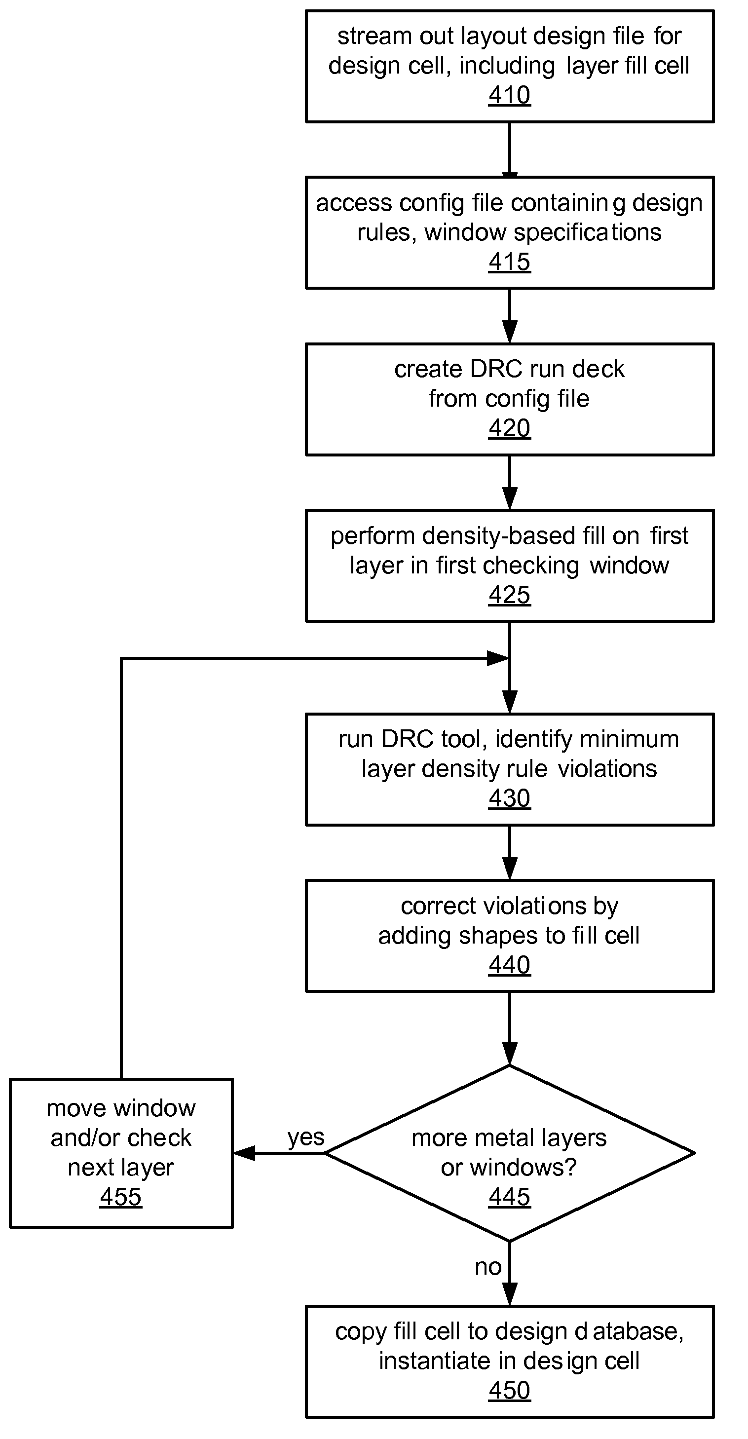
[0028]In modern deep submicron processes, chemical-mechanical polishing (CMP) may be performed during wafer processing to achieve planarity (i.e., to smooth the upper surface of the wafer between some processing steps.) This polishing is most effective when the density of features on one or more layers in the area being polished is relatively uniform. For example, uneven erosion due to CMP may be avoided by distributing features as evenly as possible across the design, rather than by having some densely-populated regions and other sparsely-populated regions on the same die. In addition, delamination or lifting of metal during CMP may be avoided when metal density is relatively uniform across the area being polished.

[0029]For these and other reasons, deep submicron processes may include design rules specifying the minimum allowed density of a given design layer within a specified area of a design. The minimum density may be heavily dependent on the particular process technology (e.g....


PUM


Abstract

A system and method for performing density-based layer filling on a design layout encoding of an integrated circuit device is disclosed. In some embodiments, the density-based layer filler may identify open areas on a given design layer in which one or more minimum density rules are not met and may insert dummy shapes only in those identified areas. The dummy shapes may be constructed so as not to violate one or more other design rules. The density-based layer filler may access a configuration file comprising layer density rules and other design rules and may generate a run deck dependent on the contents of the configuration file. The density-based layer filler may be applied iteratively to a design in checking windows of various sizes according to multiple window sizes and step values specified in the configuration file. The dummy shapes may be electrically connected to an existing ground wire after insertion.

Description

BACKGROUND OF THE INVENTION[0001]1. Field of the Invention[0002]This invention relates to integrated circuit design and more specifically to computer aided design layout and ensuring compliance with layer-density rules in a design layout in preparation for fabrication.[0003]2. Description of the Relevant Art[0004]Design of an electronic circuit, for example, an integrated circuit (IC), is a complicated and time-consuming process. FIG. 1 illustrates a typical design flow of an integrated circuit device from conception through the generation of a fabrication ready design layout. Generally, the design flow commences with defining the design specifications or requirements, such as required functionality and timing, as indicated at 110. The requirements of the design are implemented, for example, as a net-list or electronic circuit description, as indicated at 120. The implementation can be performed by, for example, schematic capture (drawing the design with a computer aided design tool...

Claims


Application Information

Patent Timeline
Patent Type & Authority Applications(United States)
IPC IPC(8): G06F17/50
CPCG06F17/5081G06F17/5068G06F30/39G06F30/398
Inventor HOEROLD, STEPHAN
Owner ORACLE INT CORP
Why Eureka
Try Eureka