Method to generate airgaps with a template first scheme and a self aligned blockout mask

a template first scheme and mask technology, applied in the field of methods, can solve the problems of poor mechanical strength, inability to achieve larger-scale copper wiring levels, and reliability issues in the final devi

Inactive Publication Date: 2008-05-29
GLOBALFOUNDRIES INC
View PDF11 Cites 34 Cited by
  • Summary
  • Abstract
  • Description
  • Claims
  • Application Information

AI Technical Summary

Benefits of technology

[0014]The invention includes a method to produce an airgap on a substrate comprising a dielectric layer on the substrate, a pattern transferred onto the dielectric layer using a self aligned block out mask which prevents etch of the dielectric layer in the blockout regions

Problems solved by technology

There are many known techniques for lowering the effective dielectric constant for the dielectrics used in semiconductor devices, however most of these methods suffer from several drawbacks including poor mechanical strength.
This poor mechanical strength results in reliability issues in the final device.
However, problems exist with this method.
For example, it is not readily practicable for larger dimension copper wiring levels.
Although these perforations may be plugged by the subsequent pinchoff deposition of an additional cap dielectric material, there may be excessive copper sputtered through the perforations, and possibly integration defects associated with these copper and copper / cap interface exposures.
Another potential problem is scaling to very large dimension wiring levels due to increased aspect ratios for nanocolumn etching, assuming the sublithographic mask perforations could not be scaled accordingly.
However, the main drawback of this method is that the depth and extent to which the UV or the electron-beam demethylates damages the SiCOH dielectric and the damaged dielectric may extend all the way to the depth of the trench.
This method has several drawbacks including problems of excess topography in the next level after dielectric deposition which requires added chemically-mechanically polished touchup or changes to the interlayer dielectric process as well as excess redeposition in airgaps, and in the extreme, pinch-off points which are so high that they can interfere with trenches on the subsequent wiring level.
Additionally, in this method, there will be situations where there are several levels of dielectric and pinch-off airgap that can be stacked on top of each other without any intervening compressive film to break up the buildup of tensile stress with the result that this structure is mechanically unstable.
Finally, this method does not scale well with shrinking dimensions and airgaps at the thin wire level using aggressive shrink factors and cannot easily be fabricated using it due to the fact that there will be exposed copper along the entire length of an interconnect during the etchback resulting in electromigration failures during reliability stressing.

Method used


Image

  • Method to generate airgaps with a template first scheme and a self aligned blockout mask
  • Method to generate airgaps with a template first scheme and a self aligned blockout mask
  • Method to generate airgaps with a template first scheme and a self aligned blockout mask

Examples


example 1

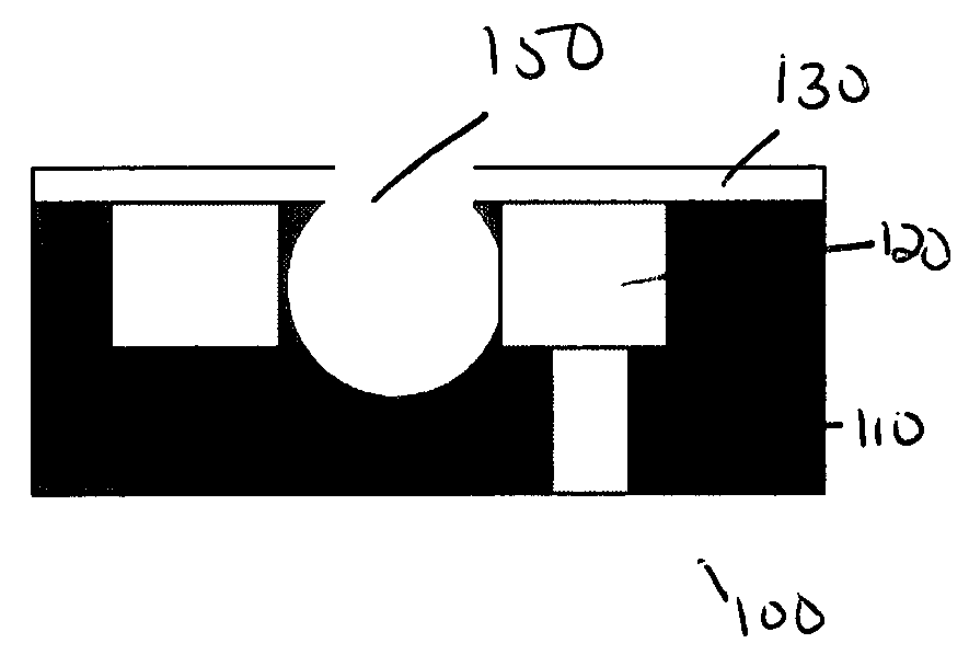
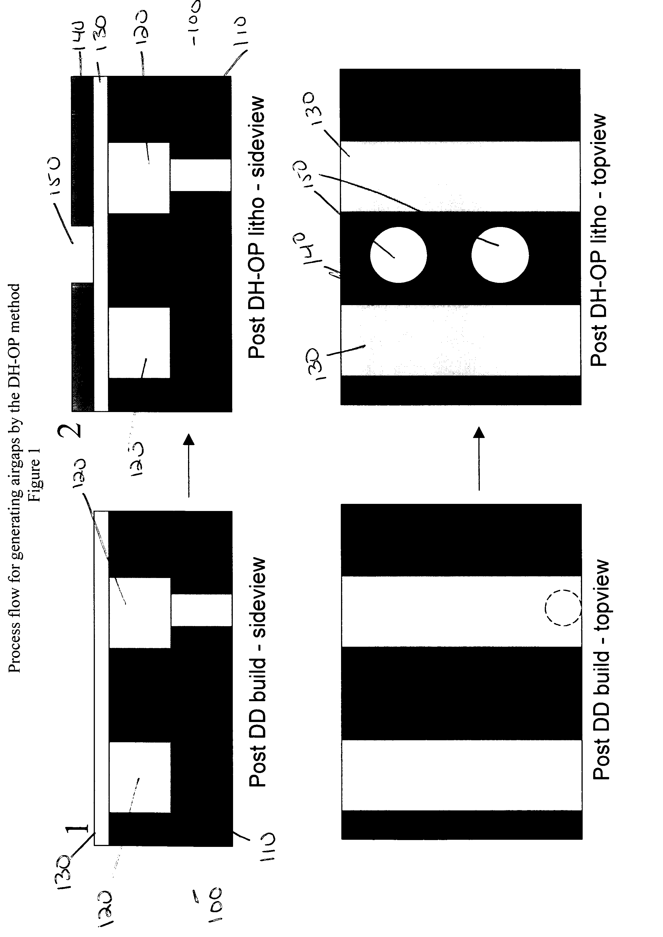
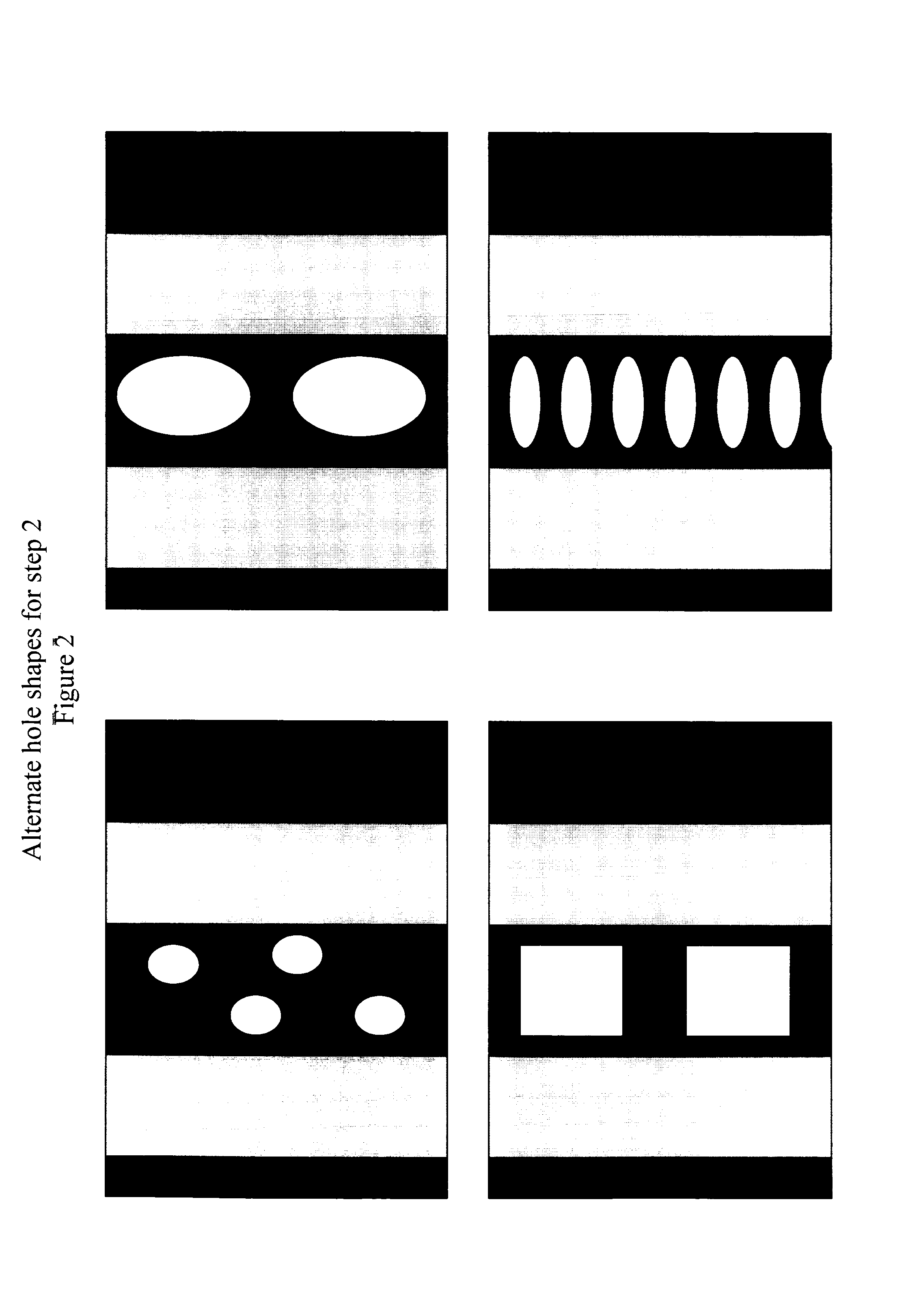
[0038]The desired interlevel dielectric on a semiconductor substrate was processed through a standard dual damascene scheme all the way to the deposition of the post-chemically-mechanically polished cap or thin hardmask. Following this, an antireflective coating and a standard 193 or 248 nm resist layer was coated on to the cap layer. A blockout mask, with perforations at least 50 nm or larger, was employed to print openings into the resist layer. Subsequently, the openings were transferred into the cap layer only. DHF was used as an etchant to etch out and remove the dielectric underneath the cap and leave behind a complete gap beneath a perforated cap. Finally, the openings in the cap were pinched-off during the deposition of the next level dielectric with very short pinch-off heights that are on the order of the perforation sizes and little or no topography at the top of the dielectric.

example 2

[0039]The desired interlevel dielectric on a semiconductor substrate was processed through a standard dual damascene scheme all the way to the deposition of the post-chemically-mechanically polished cap or thin hardmask. An antireflective coating and a standard 193 or 248 nm resist layer is coated on to the cap layer. A blockout mask with perforations that are at least 50 nm or larger is employed to print openings into the resist layer. The openings are transferred into and through the cap layer and into the underlying dielectric such that the openings are at least as deep as, or, preferably at least 25% deeper than the height of the interconnect wire. An oxidizing ash step is employed to remove the resist and further demethylate the remaining dielectric pillars if necessary. DHF is used as an etchant to remove the dielectric pillars underneath the cap and leave behind a complete gap beneath a perforated cap. Finally, the openings in the cap are pinched-off during the deposition of ...

example 3

[0040]The desired interlevel dielectric on a semiconductor substrate was processed through a standard dual damascene scheme all the way to the deposition of the post-chemically-mechanically polished cap or thin hardmask. An antireflective coating and a standard 193 or 248 nm resist layer is coated on to the cap layer. A blockout mask with perforations that are at least 50 nm or larger is employed to print openings into the resist layer. A conformal, thin, low temperature oxide layer is deposited such that the perforation openings are reduced by the thickness of the oxide layer. The oxide layer can be about 5 nm to 25 nm thick such that if the initial perforations are 75 nm in diameter, the diameter is reduced to about 65 to 25 nm respectively thus ensuring that the perforation sizes are sub-lithographic.

[0041]The openings are transferred into and through the cap layer and into the underlying dielectric such that the openings are at least as deep as, or, preferably at least 25% deepe...


PUM


Abstract

A structure and method to produce an airgap on a substrate having a dielectric layer with a pattern transferred onto the dielectric layer and a self aligned block out mask transferred on the dielectric layer around the pattern.

Description

FIELD OF THE INVENTION[0001]The present invention relates to a method of producing air gap-containing metal-insulator interconnect structures for Very Large Scale Integrated (VLSI) and Ultra-Large Scale Integrated (ULSI) devices.BACKGROUND OF THE INVENTION[0002]There are many known techniques for lowering the effective dielectric constant for the dielectrics used in semiconductor devices, however most of these methods suffer from several drawbacks including poor mechanical strength. This poor mechanical strength results in reliability issues in the final device.[0003]For example, one methodology for creating insulator voids (gaps, airgaps, etc.) in dielectric materials embedded in multilevel integrated interconnect structures to lower the effective dielectric constant includes the combination of supra-lithographic plus sub-lithographic masking to create selectively blocked-out nanocolumns or airgaps in an already-built wiring level as disclosed in US2005 / 0167838A1. The method includ...

Claims


Application Information

Patent Timeline
Patent Type & Authority Applications(United States)
IPC IPC(8): H01L23/52H01L21/4763
CPCH01L21/7682
Inventor NITTA, SATYANARAYANA VENKATAPURUSHOTHAMAN, SAMPATHCOLBURN, MATTHEW E.EDELSTEIN, DANIEL C.PONCTH, SHOM
Owner GLOBALFOUNDRIES INC
Why Eureka
Try Eureka