

Laminated electronic component and method for manufacturing the same
a technology of laminated electronic components and manufacturing methods, which is applied in the direction of fixed capacitor details, variable capacitors, fixed capacitors, etc., can solve the problems of cumbersome process for adding catalysts, reduced effective volume rate of laminated bodies, and significant reduction of reliability of laminated bodies, etc., to achieve high effective volume rate
- Summary
- Abstract
- Description
- Claims
- Application Information
AI Technical Summary
Benefits of technology
Problems solved by technology
Method used
Image

Examples
experimental example 1
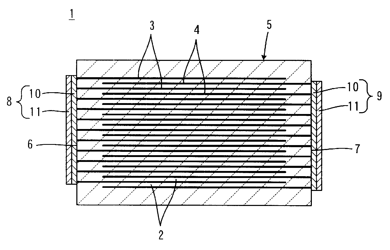
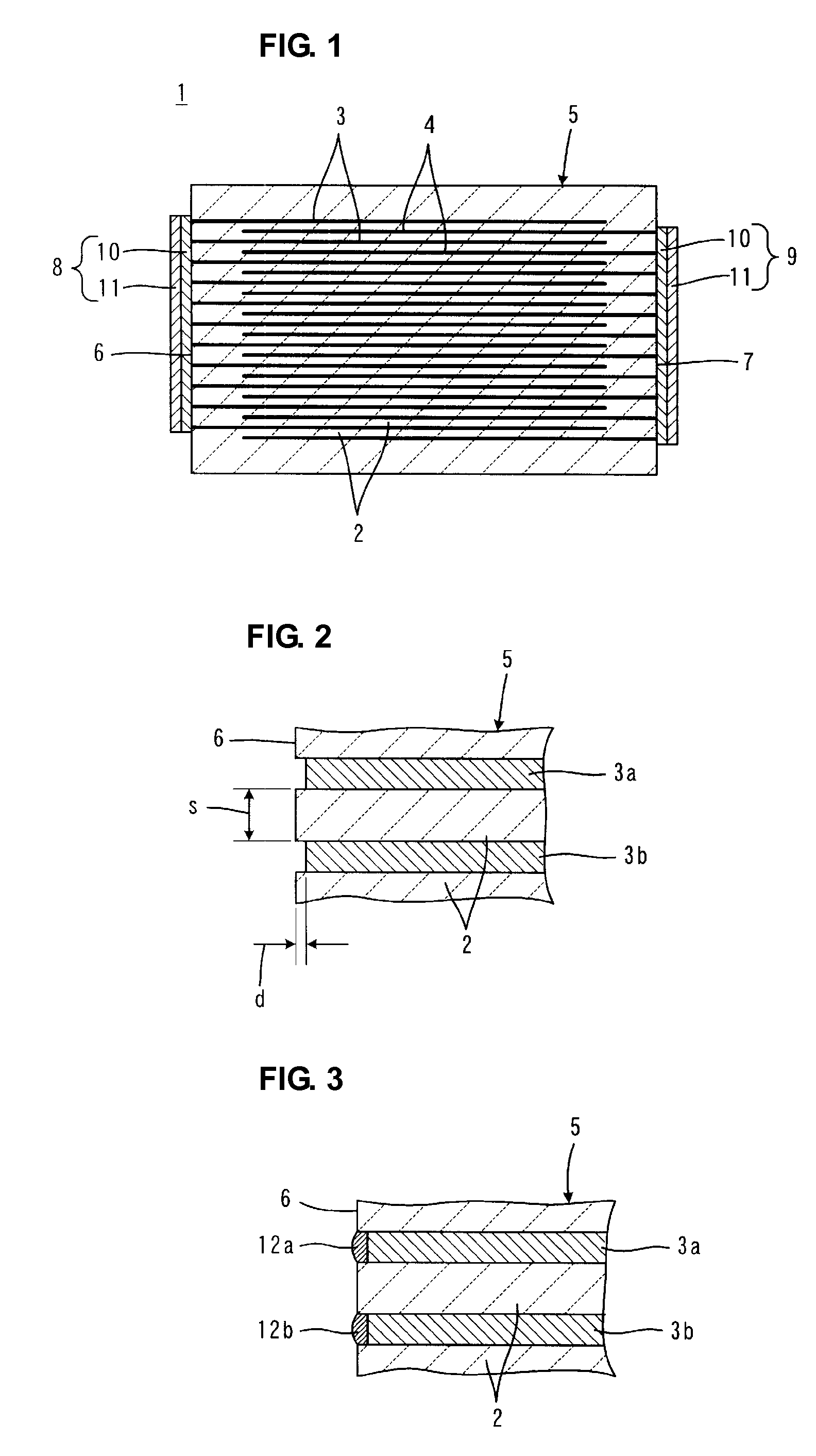
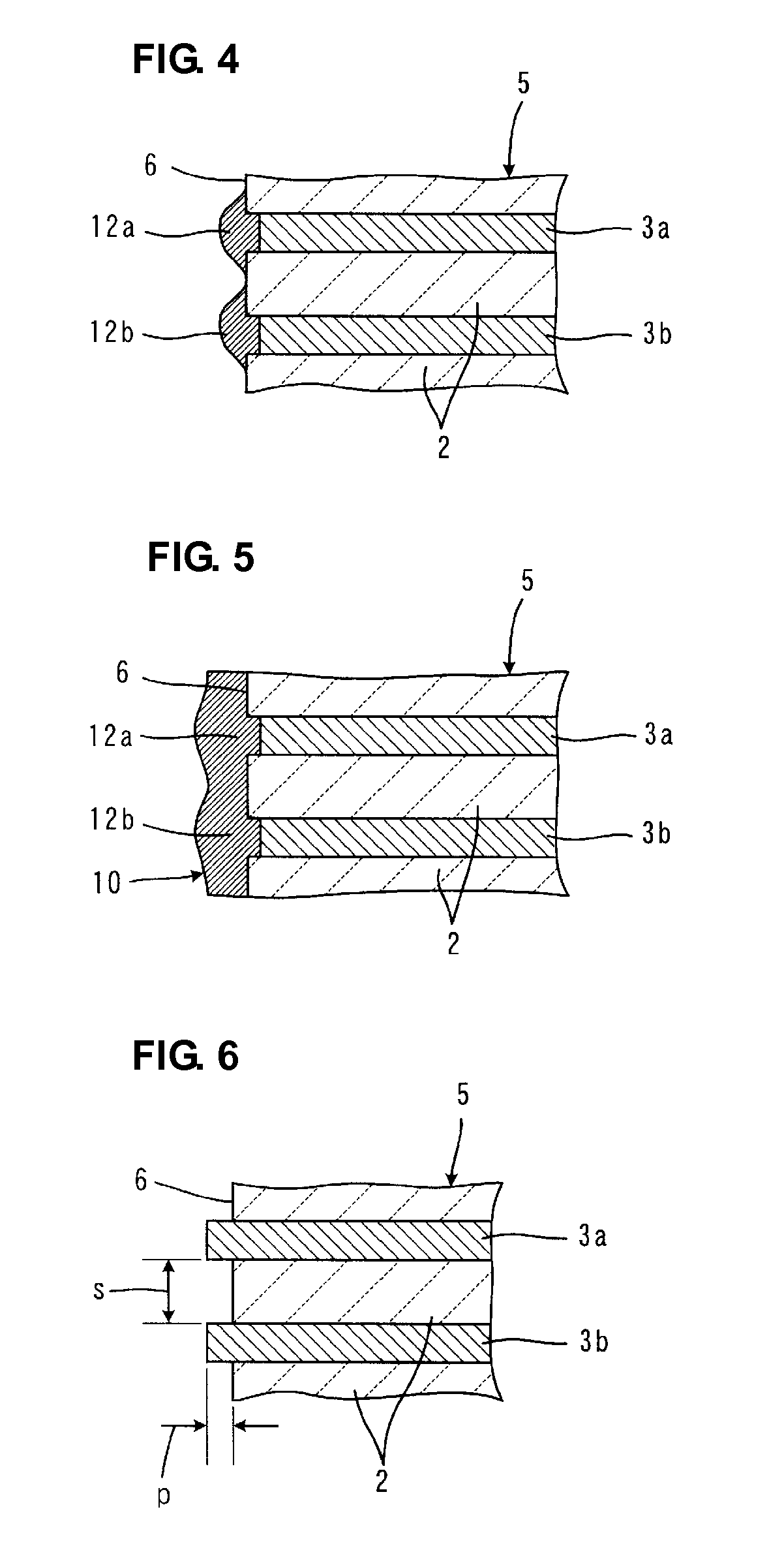
[0094]In EXPERIMENTAL EXAMPLE 1, several modified laminated bodies that are modifications of a laminated body for a laminated electronic component shown in FIG. 1 were prepared. Each modified laminated body included different distances “s” between internal electrodes (i.e., the thickness of the insulator layer) and withdrawn-depths “d” or a protrusion lengths “p,” which are shown in FIGS. 2 and 6. A Ni plating layer was formed directly on each of end surfaces and a Sn plating layer was formed on the Ni plating layer. Through these processes, the performance of the plating process was investigated.
[0095]More specifically, samples of the laminated bodies defining laminated ceramic capacitors were prepared for plating. The samples have a length of about 1.6 mm, a width of about 0.8 mm, and a thickness of about 0.8 mm and have an insulator layer made of a barium titanate dielectric material. The thicknesses of the insulator layer and each of the internal electrodes, and a main component...
experimental example 2
[0105]In Experimental Example 2, an influence of the thickness of the internal electrodes of the laminated bodies under certain conditions of samples and plating was investigated.
[0106]All samples of laminated bodies include insulator layers having a thickness of about 20 μm and the internal electrodes made of Ni as a main component. The thickness of the internal electrodes of the samples was varied as shown in “Thickness of Internal Electrode” of Table 3 and other conditions of the samples of the laminated bodies were the same as those used in as Experimental Example 1.
[0107]Next, laminated bodies of Samples 11 to 13 alone were sandblasted with the same abrasive as used in Experimental Experiment 1 and a withdrawn-depth “d” from an end surface of the laminated body having the internal electrodes exposed thereon to end portions of the internal electrodes was adjusted to be about 0.1 μm.
[0108]Next, 5,000 pieces of the above-mentioned laminated bodies were immersed in a rotation barre...
experimental example 3
[0115]In Experimental Example 3, a first plating layer was formed using various plating metal ions under various plating conditions.
[0116]All samples of laminated bodies include insulator layers having a thickness of 20 μm and internal electrodes having a thickness of 0.6 μm. A main component of the internal electrodes of the samples was varied as shown in “Metal Type of Internal Electrode” of Table 4 and other conditions of the samples of the laminated bodies were the same as used in Experimental Example 1.
[0117]Next, the laminated bodies were sandblasted with the same abrasive as used in Experimental Experiment 1 and withdrawn-depth “d” from an end surface of the laminated bodies having the internal electrodes exposed thereon to end portions of the internal electrodes was adjusted to be 0.1 μm.
[0118]Next, 5,000 pieces of the above-mentioned laminated bodies were immersed into a rotation barrel with a volume of 300 cc. As shown in “Plating Condition” of Table 4, under the condition...
PUM
| Property | Measurement | Unit |
|---|---|---|
| Length | aaaaa | aaaaa |
| Length | aaaaa | aaaaa |
| Length | aaaaa | aaaaa |
Abstract
Description
Claims
Application Information