Method for Modeling an HDL Design Using Symbolic Simulation

a symbolic simulation and design technology, applied in the field of symbolic simulation of hdl design, can solve the problems of system well beyond the capacity of human designers, need to validate such a circuit, and designer's necessity to construct simulation routines

Active Publication Date: 2008-05-29
SYNOPSYS INC
View PDF5 Cites 9 Cited by
  • Summary
  • Abstract
  • Description
  • Claims
  • Application Information

AI Technical Summary

Benefits of technology

[0006]A method for digital circuit design. The first step of the process is the step of providing a circuit design in the form of a hardware definition language. Then, the process produces a binary simulation of the design by setting out for each unit of time during execution of the hardware design a contr...

Problems solved by technology

Such systems are well beyond the capacity of human designers.
A major issue, however, is the need to validate such a circuit.
The primary weakness of concrete simulation is the necessity for a designer to construct the simulation routines.
Given the complexity of a modern digital circuit, no system could run all possible inputs, and no designer could list them.
Of course, simulation of a complex circuit proceeds at a relatively slow pace, given the need to determine and record operations ac...

Method used


Image

  • Method for Modeling an HDL Design Using Symbolic Simulation
  • Method for Modeling an HDL Design Using Symbolic Simulation
  • Method for Modeling an HDL Design Using Symbolic Simulation

Examples


Embodiment Construction

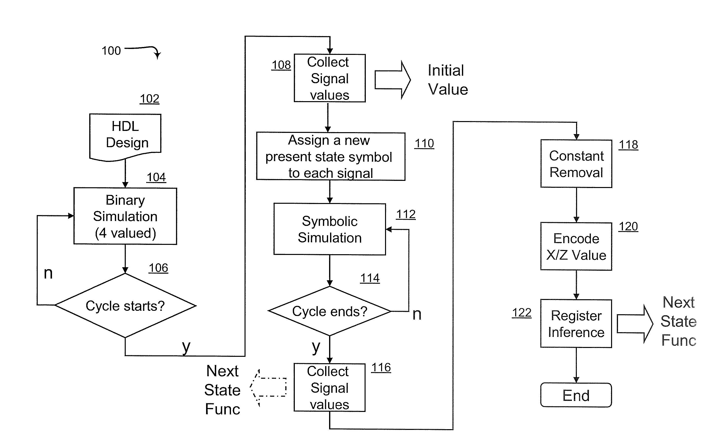
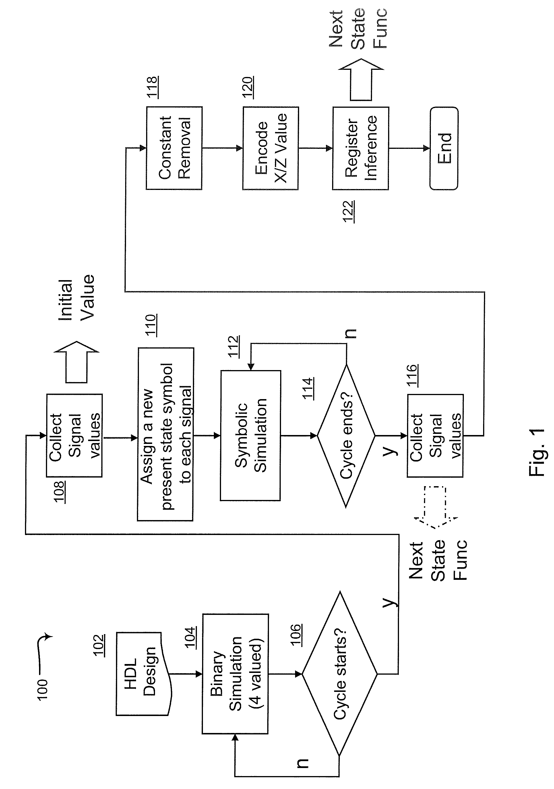
[0009]The following detailed description is made with reference to the figures. Preferred embodiments are described to illustrate the present invention, not to limit its scope, which is defined by the claims. Those of ordinary skill in the art will recognize a variety of equivalent variations on the description that follows.

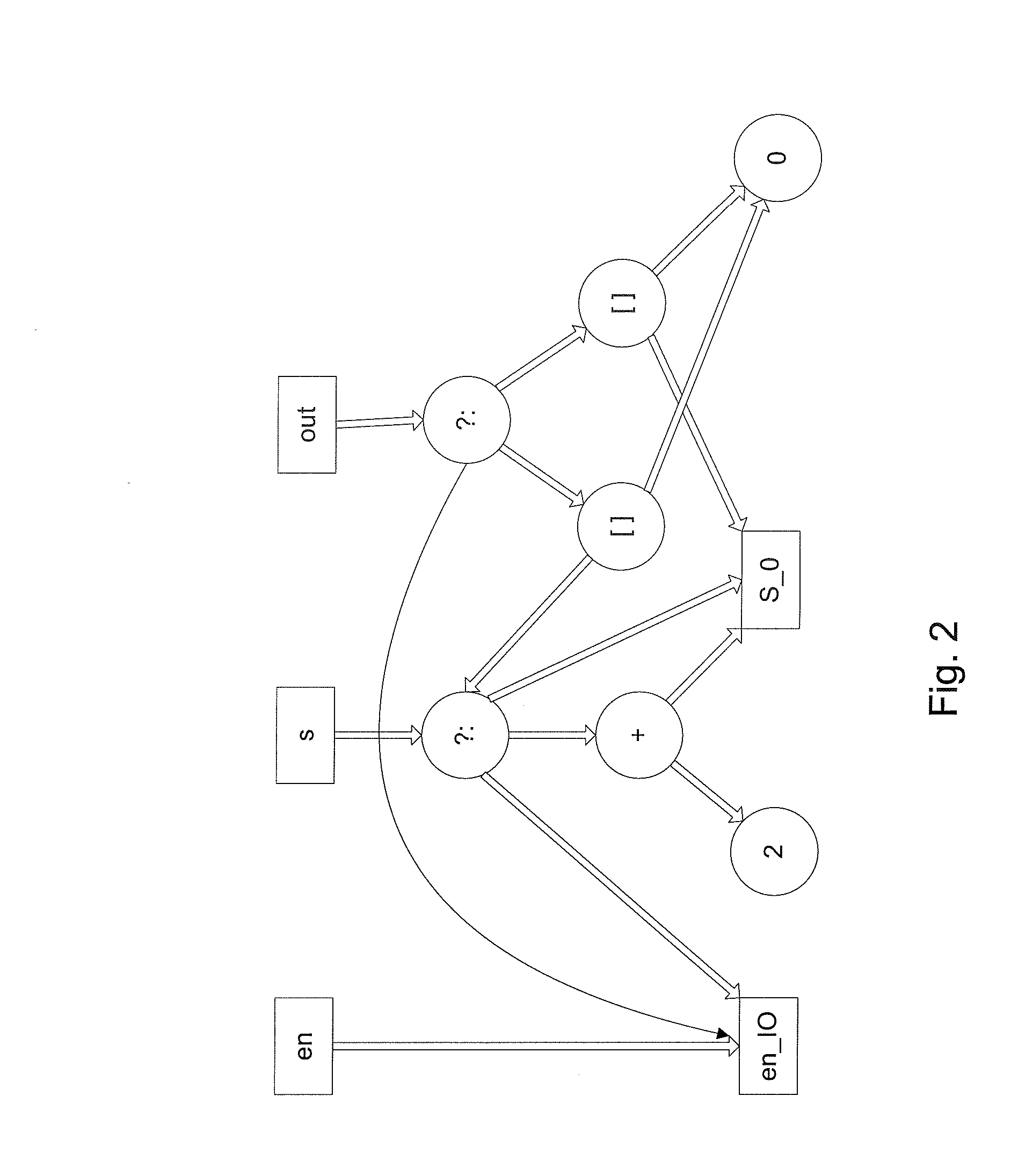
[0010]An exemplary embodiment sets out the symbolic simulation off the Verilog design shown in Table 1, below. As seen, that design describes a 4-bit counter s, having an output signal par, which depends of the value of input signal even, computes whether the parity of the count is odd or even. Two threads are set out, one of which performs the count and the other computes the parity bit.

TABLE 1Counter with parity bitD1 : module dut(clk, rst, even, par);D2 : input clk, rst, even; output par;D3 : reg [3:0] s; reg par;D4 :D5 : always @(posedge clk or posedge rst)D6 :  if (rst) s D7 :  else  s D8 :D9 : always @(s or even) beginD10:  #5;D11:  par = even & {circumflex...


PUM


Abstract

A method for digital circuit design. The first step of the process is the step of providing a circuit design in the form of a hardware definition language. Then, the process produces a binary simulation of the design by setting out for each unit of time during execution of the hardware design the a control state and a program state of the design and assigns a symbol to each signal of the design. The process proceeds by executing a symbolic simulation of the design, concluding with identifying and capturing the combinational logic expression of the simulation output and the next state functions of the simulation.

Description

BACKGROUND OF THE INVENTION[0001]Design of modern digital circuits is accomplished with electronic design automation (EDA) tools, capable of dealing with component arrays that total millions of gates. Such systems are well beyond the capacity of human designers. Generally, an EDA tool must be able to accept as input a functional description of a given circuit, and it must produce as output a concrete circuit design. The art has largely relied on hardware design languages (HDLs) to perform automated electronic design functions. Languages such as Verilog or VHDL can express designs either at gate level or at Register Transfer Level (RTL). After the design is rendered in RTL, the design is translated into a combinational netlist, which can serve as a blueprint for rendering the circuit in silicon.[0002]A major issue, however, is the need to validate such a circuit. Not only must the designer be confident of the ability of the circuit to operate without electronic, timing or interconnec...

Claims


Application Information

Patent Timeline
IPC IPC(8): G06F17/50
CPCG06F17/504G06F30/3323
Inventor ZHU, YUNSHANKUKULA, JAMES HERBERTDAMIANO, ROBERT F.BUCK, JOSEPH T.
Owner SYNOPSYS INC
Why Eureka
Try Eureka