Alignment of a cap to a MEMS wafer

a technology of printed caps and mems wafers, applied in the field of microelectromechanical systems, can solve the problems of too large design patterns, and achieve the effects of reducing alignment tolerances, repeatable and accurate alignment bonding process, and reducing alignment tolerances

Inactive Publication Date: 2008-06-05
DELPHI TECH INC
View PDF5 Cites 18 Cited by
  • Summary
  • Abstract
  • Description
  • Claims
  • Application Information

AI Technical Summary

Benefits of technology

[0004]An apparatus and method is provided that accurately aligns a cap wafer relative to a microelectromechanical systems (MEMS) wafer. The method may further be used to precisely situate materials other than a cap and MEMS wafer in a predetermined location, such as those used with integrated circuit microchips and nanotechnology devices. During the bonding process, the present invention cap wafer shifts toward proper alignment, rather than away from an initial alignment point as in many conventional systems. The alignment tolerances required conventionally (i.e., 1 to 2 mils) during the device design stage are decreased, since the present invention provides a repeatable and accurate alignment bonding process. The decreased alignment tolerance results in increased chip multiple and therefore decreased chip cost.

Problems solved by technology

Further, in an example, a screen printer forms the substance pattern in a limited range of dimensions, which may be too large for the needed design pattern.

Method used


Image

  • Alignment of a cap to a MEMS wafer
  • Alignment of a cap to a MEMS wafer
  • Alignment of a cap to a MEMS wafer

Examples


Embodiment Construction

[0020]Exemplary embodiments are described with reference to specific configurations. Those of ordinary skill in the art will appreciate that various changes and modifications can be made while remaining within the scope of the appended claims. Additionally, well-known elements, devices, components, methods, process steps and the like may not be set forth in detail in order to avoid obscuring the invention. Further, unless indicated to the contrary, the numerical values set forth in the following specification and claims are approximations that may vary depending upon the desired characteristics sought to be obtained by the present invention.

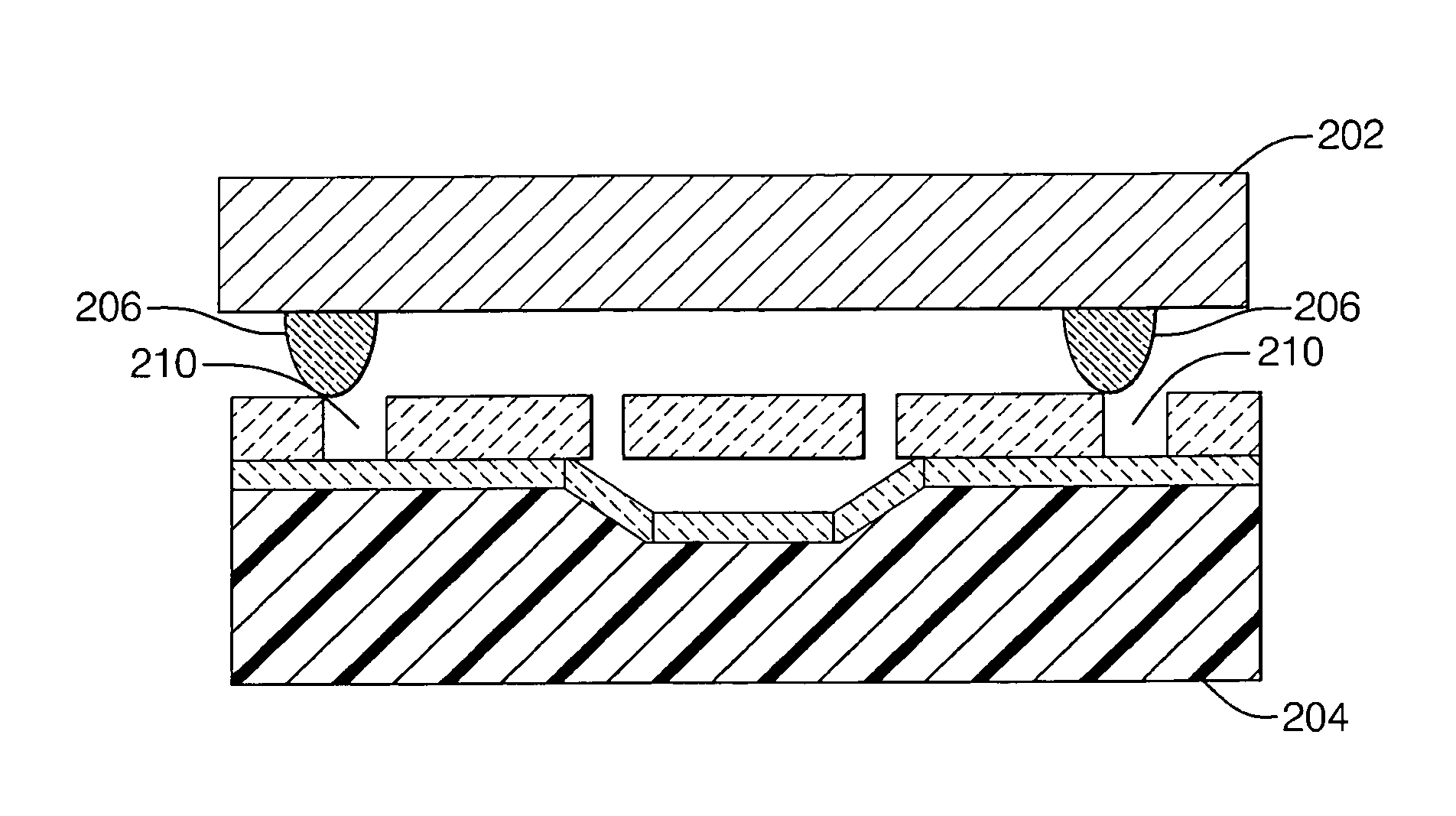
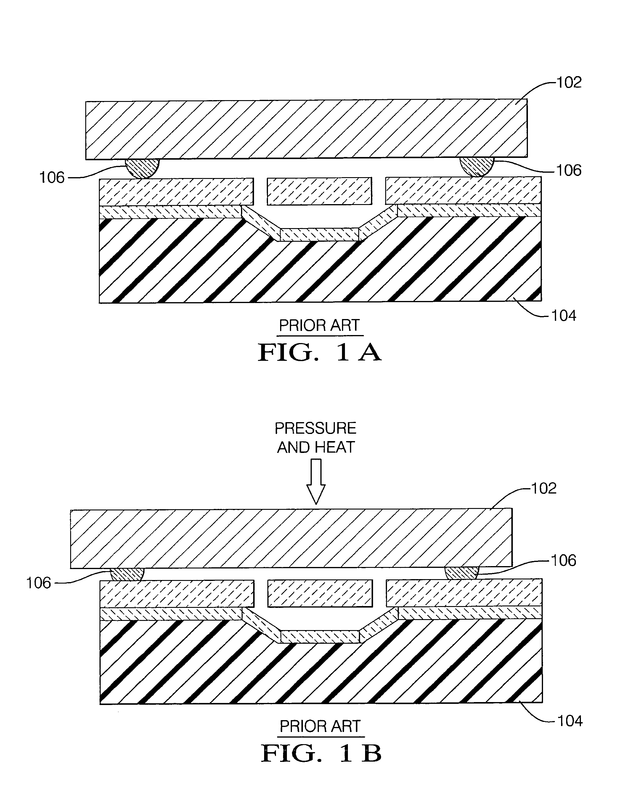
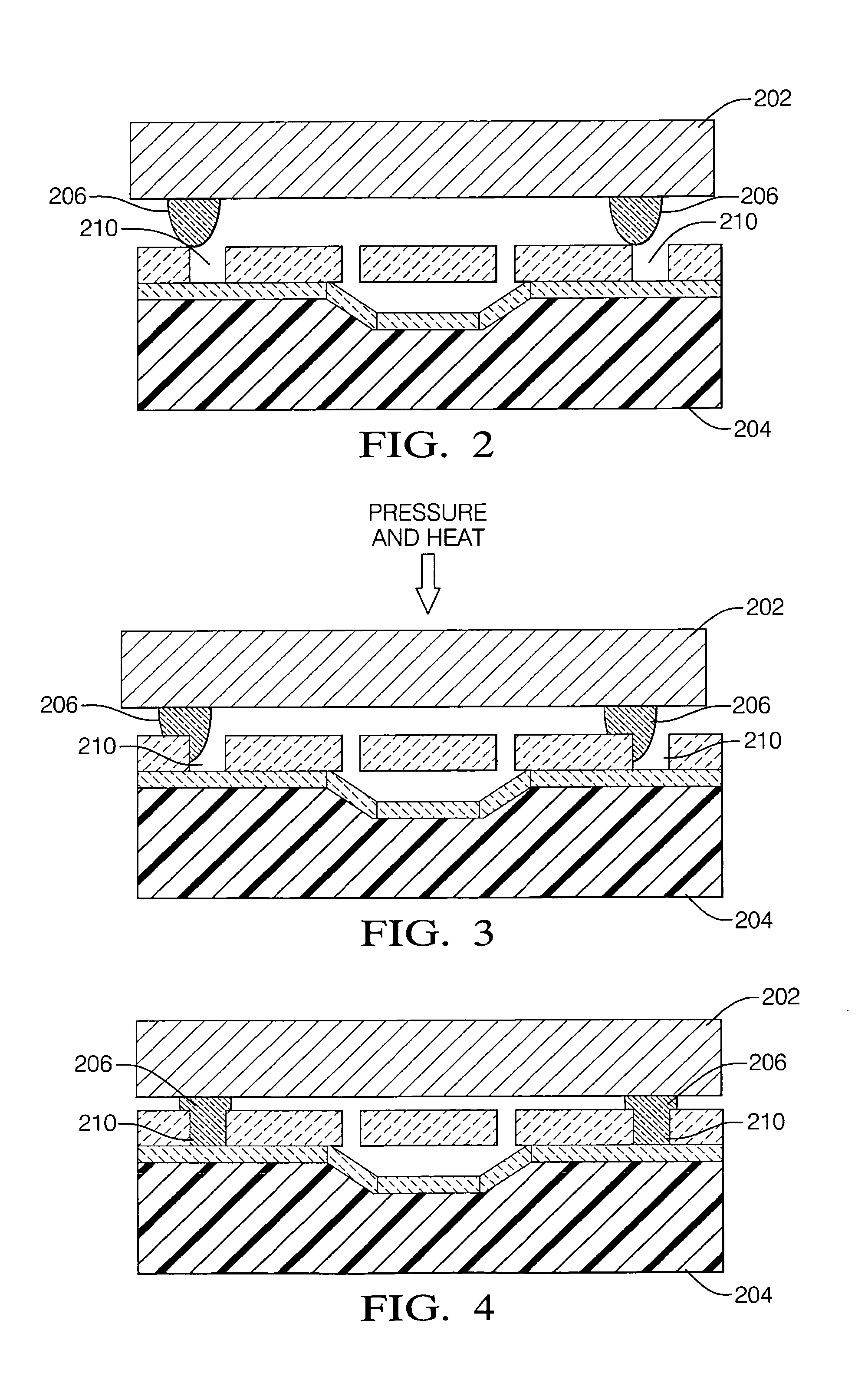
[0021]In microelectromechanical systems (MEMS) applications, a cap wafer is often bonded to a MEMS device wafer by utilizing a glass frit bonding material. In some applications, such as an accelerometer, a hermetic seal is established. Referring to the drawings wherein identical reference numerals denote the same elements throughout the various v...


PUM

PropertyMeasurementUnit
widthaaaaaaaaaa
widthaaaaaaaaaa
distanceaaaaaaaaaa

Abstract

An apparatus and method is provided to accurately align a cap wafer relative to a microelectromechanical systems (MEMS) wafer during a bonding process. Other materials may be accurately aligned as well. A trench is established in the MEMS wafer, and a printed substance, secured to the cap wafer, flows into the trench when a pressure is applied to the cap wafer at bond temperature. Natural forces aid in shifting the materials into a lowest energy state and self-aligns the materials into a desired position. The trench also serves as a collection trench for the flowing substance by helping to shape the substance. The trench dimensions may be used to aid in creating a hermetic seal. The alignment tolerances required conventionally during the device design stage are decreased, since the present invention provides a repeatable and accurate alignment bonding process. Chip multiple is increased and therefore chip costs are decreased.

Description

FIELD OF THE INVENTION[0001]The invention relates generally to microelectromechanical systems (MEMS), and more particularly to accurately aligning a frit printed cap wafer relative to a MEMS wafer.BACKGROUND OF THE INVENTION[0002]Microelectromechanical systems (MEMS) are devices that use microfabrication technology to develop mechanical elements linked to electrical components for detection and actuation. MEMS devices are widely used, with common applications including biotechnology, communications, piezoelectrics, accelerometers for collision airbag deployment, pressure sensors, and optical switching. These devices generally range in size from a micrometer to a millimeter. MEMS devices are thus typically manufactured using planar processing similar to semiconductor processes such as surface micromachining and / or bulk micromachining. MEMS technology is implemented using a wide range of different materials and manufacturing techniques, depending on the device being created. Materials...

Claims


Application Information

Patent Timeline
Patent Type & Authority Applications(United States)
IPC IPC(8): B32B3/26B05D5/12B05D3/12
CPCB81C1/00269B81C3/002Y10T428/24355B81C2203/032B81C2203/058B81C2203/0118
Inventor JORDAN, LARRY L.JORDAN, KAYDIBIASO, HEATHER H.
Owner DELPHI TECH INC
Why Eureka
Try Eureka