Methods and systems for controlling a semiconductor fabrication process

a technology for manufacturing process and semiconductor, applied in the direction of program control, total factory control, instruments, etc., can solve the problems of proprietary or pre-compiled software unsuitable for a newly conceived process, significant computing challenges for the handling of workpieces such as wafers in the semiconductor manufacturing environment, etc., to achieve the effect of improving usability and computational efficiency

Inactive Publication Date: 2008-06-05
BOOKS AUTOMATION US LLC
View PDF4 Cites 20 Cited by
  • Summary
  • Abstract
  • Description
  • Claims
  • Application Information

AI Technical Summary

Benefits of technology

[0008]Software for controlling processes in a heterogeneous semiconductor manufacturing environment may include a wafer-centric database, a real-time scheduler using a neural network, and a graphical user interface displaying simulated operation of the system. These features may be employed alone or in combination to offer improved usability and computational efficiency for real time control and monitoring of a semiconductor manufacturing process. More generally, these techniques may be usefully employed in a variety of real time control systems, particularly systems requiring complex scheduling decisions or heterogeneous systems constructed of hardware from numerous independent vendors.
[0014]At least one of the plurality of states may represent a state of an item of hardware within the semiconductor manufacturing system. At least one of the states may represent a position of a workpiece within the semiconductor manufacturing system. At least one of the states may represent a position of an isolation valve within the system. The computer executable code may further perform the step of updating the neural network in substantially real time. The computer executable code may further perform the step of updating the neural network every 20 milliseconds. The inputs to the neural network may include one or more of sensor data, temperature data, a detected workpiece position, an estimated workpiece temperature, an actual workpiece temperature, a valve state, an isolation valve state, robotic drive encoder data, robotic arm position data, end effector height data, a process time, a process status, a pick time, a place time, and a control signal. The inputs to the neural network may include at least one process time for a workpiece within the semiconductor manufacturing system. The at least one process time may include one or more of a target duration, a start time, an end time, and an estimated end time. The inputs may include a transition time. The transition time may include one or more of a pump down to vacuum time and a vent to atmosphere time. At least one of the states includes a transition to itself. The computer executable code may further perform the step of updating the state machine in substantially real time. The computer executable code may further perform the step of updating the state machine every 20 milliseconds. The computer executable code may further perform the step of controlling operation of a semiconductor manufacturing system with a plurality of state machines, each one of the plurality of state machines controlling a portion of the semiconductor manufacturing system according to one of a plurality of neural networks.

Problems solved by technology

The handling of workpieces such as wafers within a semiconductor manufacturing environment can present significant computing challenges.
Hardware such as process modules, handlers, valves, robots, and other equipment are commonly assembled from a variety of different manufacturers each of which may provide proprietary or pre-compiled software unsuitable for a newly conceived process.

Method used


Image

  • Methods and systems for controlling a semiconductor fabrication process
  • Methods and systems for controlling a semiconductor fabrication process
  • Methods and systems for controlling a semiconductor fabrication process

Examples


Embodiment Construction

[0043]The systems and methods described herein relate to software for operating a semiconductor manufacturing system. While the following example embodiments are directed generally to semiconductor fabrication, it will be understood the that the principles disclosed herein have broader applicability, and may be usefully employed, for example, in any industrial control environment, particularly environments characterized by complex scheduling, control of robotic components, and / or real time processing based upon system states, sensor feedback, and the like.

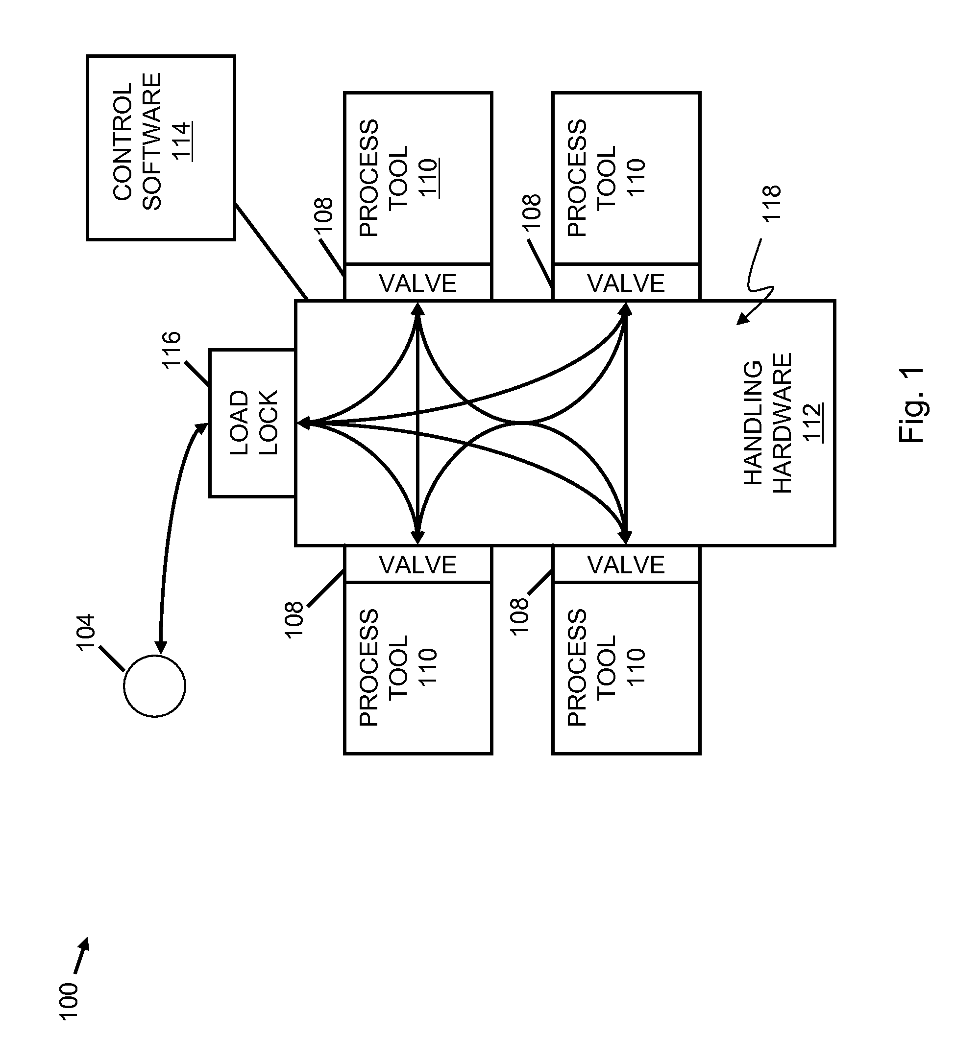
[0044]FIG. 1 shows a semiconductor processing system. The system 100 for processing a wafer 104 may include a plurality of valves 108, a plurality of process tools 110, handling hardware 112, control software 114, and a load lock 116. In general operation, the system 100 operates to receive a wafer 104 through the load lock 116, to move the wafer 104 among the process tools 110 with the handling hardware 112 so that the wafer 104 m...


PUM


Abstract

Software for controlling processes in a heterogeneous semiconductor manufacturing environment may include a wafer-centric database, a real-time scheduler using a neural network, and a graphical user interface displaying simulated operation of the system. These features may be employed alone or in combination to offer improved usability and computational efficiency for real time control and monitoring of a semiconductor manufacturing process. More generally, these techniques may be usefully employed in a variety of real time control systems, particularly systems requiring complex scheduling decisions or heterogeneous systems constructed of hardware from numerous independent vendors.

Description

CROSS-REFERENCE TO RELATED APPLICATIONS[0001]This claims the benefit of U.S. App. No. 60 / 746,163 filed on May 1, 2006 and U.S. App. No. 60 / 807,189 filed on Jul. 12, 2006. This application is a continuation-in-part of U.S. application Ser. No. 10 / 985,834, filed on Nov. 10, 2004, which claims the benefit of U.S. App. No. 60 / 518,823 filed on Nov. 10, 2003 and U.S. App. No. 60 / 607,649 filed on Sep. 7, 2004. This application is also a continuation-in-part of U.S. application Ser. No. 11 / 123,966 filed on May 6, 2005, and a continuation-in-part of U.S. application Ser. No. 11 / 302,563 filed on Dec. 13, 2005.[0002]Each of the foregoing commonly-owned applications is incorporated by reference herein in its entirety.BACKGROUND[0003]1. Field[0004]This invention relates to, inter alia, methods of utilizing a wafer-centric database to improve system throughput.[0005]2. Related Art[0006]The handling of workpieces such as wafers within a semiconductor manufacturing environment can present significa...

Claims


Application Information

Patent Timeline
Patent Type & Authority Applications(United States)
IPC IPC(8): G06F3/048
CPCG05B15/02G05B2219/40424G05B19/41885G05B23/0267G05B2219/31467G05B2219/31472G05B2219/32128G05B2219/32267G05B2219/32329G05B2219/32335G05B2219/32342G05B2219/32351G05B2219/35494G05B2219/45031G06T7/0004H01L21/67161H01L21/67184H01L21/6719H01L21/67196H01L21/67201H01L21/67207H01L21/67742H01L21/67745G05B99/00G05B2219/40419G05B2219/40413G05B2219/40412G05B2219/40411G05B2219/31G05B2219/30G05B19/41865Y02P90/02Y02P90/80G06F15/00
Inventor PANNESE, PATRICK D.KAVATHEKAR, VINAYAVAN DER MEULEN, PETER
Owner BOOKS AUTOMATION US LLC
Why Eureka
Try Eureka