
RF substrate bias with high power impulse magnetron sputtering (hipims)

a high-power, magnetron-sputtering technology, applied in the field of sputtering, can solve the problems of dc bias not working on electrically insulating surfaces, arcing may occur on the substrate, wafer damage,

Active Publication Date: 2008-06-12
OERLIKON ADVANCED TECH +1
View PDF5 Cites 48 Cited by
  • Summary
  • Abstract
  • Description
  • Claims
  • Application Information

AI Technical Summary

Benefits of technology

[0010]The following presents a simplified summary of the invention in order to provide a basic understanding of some example aspects of the invention. This summary is not an extensive overview of the invention. Moreover, this summary is not intended...

Problems solved by technology

There are a number of disadvantages with the standard HIPIMS technique.
While using DC bias helps to define ion energy at a substrate, a disadvantage occurs in that arcing may occur on the substrate.
Arcing on the substrate causes wafer damage when wafer processing is used.
Another disadvantage is that DC bias also does not work on electrically insulating surfaces, such as trenches and vias using oxide materials.
Nevertheless, placing a bulky ICP coil between the magnetron and the substrate complicates the design, increases the probability of particle formation, and reduces the deposition rate due to the increased target-substrate spacing.

Method used


Image

  • RF substrate bias with high power impulse magnetron sputtering (hipims)
  • RF substrate bias with high power impulse magnetron sputtering (hipims)
  • RF substrate bias with high power impulse magnetron sputtering (hipims)

Examples


Embodiment Construction

[0030]Examples that incorporate one or more aspects of the present invention are described and illustrated in the drawings. These illustrated examples are not intended to be a limitation on the present invention. For example, one or more aspects of the present invention can be utilized in other embodiments and even other types of devices. Moreover, certain terminology is used herein for convenience only and is not to be taken as a limitation on the present invention. Still further, in the drawings, the same reference numerals are employed for designating the same elements.

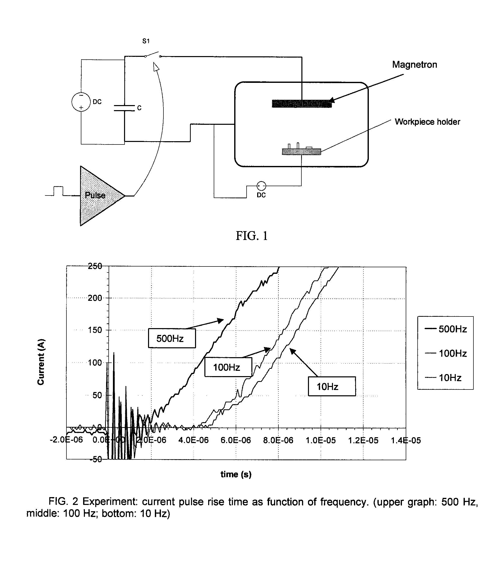
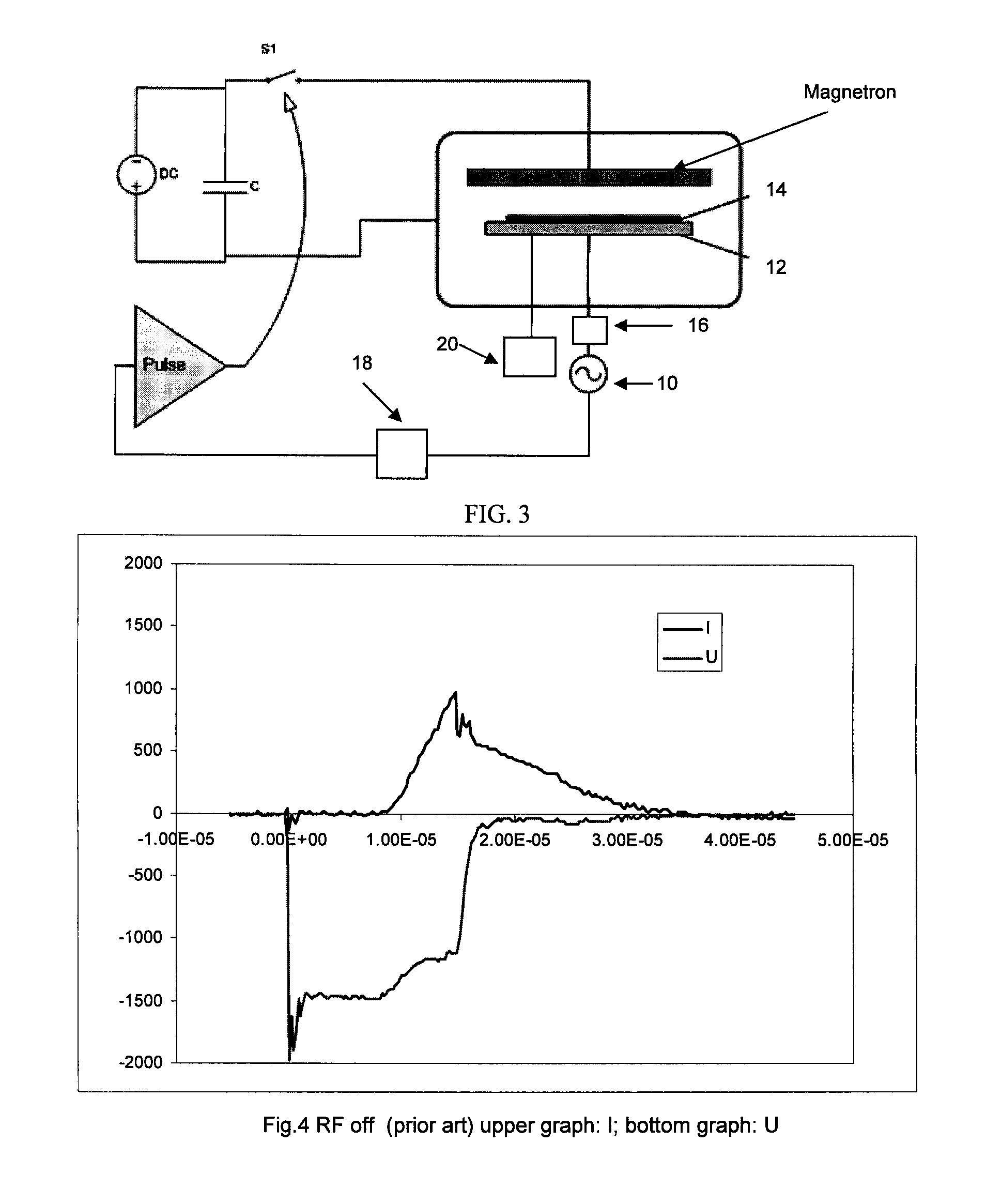
[0031]FIG. 3 shows a first example schematic of the subject invention. For example, the invention can use standard HIPIMS wiring, such as the wiring in FIG. 1, but in addition, an electrical bias device 10, such as an RF generator, is connected to a substrate 14. For example, the electrical bias device can be connected to a chuck 12 that holds the substrate 14. This first example can include a magnetron including a...


PUM

PropertyMeasurementUnit
Fractionaaaaaaaaaa
Fractionaaaaaaaaaa
Timeaaaaaaaaaa

Abstract

An apparatus for generating sputtering of a target to produce a coating on a substrate with a current density on a cathode of a magnetron between 0.1 and 10 A / cm2 is provided. The apparatus comprises a power supply that is operably connected to the magnetron and at least one capacitor is operably connected to the power supply. A first switch is also provided. The first switch operably connects the power supply to the magnetron to charge the magnetron and the first switch is configured to charge the magnetron according to a first pulse. An electrical bias device is operably connected to the substrate and configured to apply a substrate bias.

Description

CROSS-REFERENCE TO RELATED APPLICATIONS[0001]This application claims the benefit of U.S. Provisional Application No. 60 / 869,912, filed Dec. 14, 2006, the entire disclosure of which is hereby incorporated herein by reference. This application also claims the benefit of U.S. Provisional Application No. 60 / 869,566, filed Dec. 12, 2006, the entire disclosure of which is hereby incorporated herein by reference. This application also claims the benefit of U.S. Provisional Application No. 60 / 869,578, filed Dec. 12, 2006, the entire disclosure of which is hereby incorporated herein by reference.BACKGROUND OF THE INVENTION[0002]The present invention relates generally to sputtering, and more particularly, to high power impulse magnetron sputtering (HIPIMS).[0003]Sputtering is a physical process whereby atoms in a solid target material are ejected into the gas phase due to bombardment of the material by energetic ions. The process of sputtering is commonly used for thin-film deposition. The en...

Claims


Application Information

Patent Timeline
IPC IPC(8): C23C14/35
CPCH01J37/3444H01J37/3467C23C14/35C23C14/3485C23C14/345H01J37/3408H01J37/32944H01J37/32045H01J37/32064
Inventor KADLEC, STANISLAVWEICHART, JURGEN
Owner OERLIKON ADVANCED TECH
Learn More