Vertical structure led device and method of manufacturing the same

a technology of compound semiconductors and led devices, which is applied in the direction of semiconductor/solid-state device manufacturing, semiconductor devices, electrical equipment, etc., can solve the problems of reducing process yield, bending the substrate, generating a lot of defects and cracks in the gan semiconductor layer, and preventing crystal defects or cracks occurrence, the effect of improving the ohmic characteristics of the electrode conta

Active Publication Date: 2008-06-12
SAMSUNG ELECTRONICS CO LTD
View PDF4 Cites 83 Cited by
  • Summary
  • Abstract
  • Description
  • Claims
  • Application Information

AI Technical Summary

Benefits of technology

[0012]An aspect of the present invention provides a method of manufacturing a vertical structure light emitting diode device effective capable of performing wafer bonding at a low temperature of 200° C. or less, preventing crystal defects or a crack occurrence, and being effective in improving ohmic characteristics of an electrode contact.

Problems solved by technology

In the horizontal structure GaN LED device, since all of the two electrodes are disposed above the device, there are disadvantages in aspects of current diffusion and electrostatic.
In a condition of such the high temperature and high pressure, due to a difference between thermal expansion coefficients of the sapphire substrate and conductive substrate, a great stress is applied to a substrate, thereby bending the substrate or generating a lot of defects and cracks in the GaN semiconductor layer.
Particularly, in a laser lift off process after wafer bonding, a bonding structure itself is destroyed, thereby greatly reducing a process yield.
However, in the case of the wafer bonding using an eutectic metal having a low melting point as a bonding material, there is still a stress generated due to a difference between thermal expansion coefficients of a substrate for growth and a conductive substrate at a temperature from 200 to 330° C. Also, a thermal processing temperature to improve ohmic characteristics of the n-side electrode layer formed on the n-type semiconductor layer exposed after removing the substrate for growth is limited to be less than a melting point of the eutectic metal, approximately, 330° C. or more, it is difficult to obtain suitable ohmic characteristics.
The described problems due to a metal bonding material used in wafer bonding of a vertical structure LED manufacturing process may occur not only in a GaN semiconductor LED manufacturing process but also a vertical structure LED device manufacturing process using other III-V group compound semiconductor such as AlGaInP and AlGaAs semiconductors.

Method used


Image

  • Vertical structure led device and method of manufacturing the same
  • Vertical structure led device and method of manufacturing the same
  • Vertical structure led device and method of manufacturing the same

Examples


Embodiment Construction

[0030]Hereinafter, exemplary embodiments of the present invention will now be described in detail with reference to the accompanying drawings. The invention may however be embodied in many different forms and should not be construed as limited to the embodiments set forth herein. Rather, these embodiments are provided so that this disclosure will be thorough and complete, and will fully convey the scope of the invention to those skilled in the art. In the drawings, the shapes and dimensions may be exaggerated for clarity, and the same reference numerals are used throughout to designate the same or similar components.

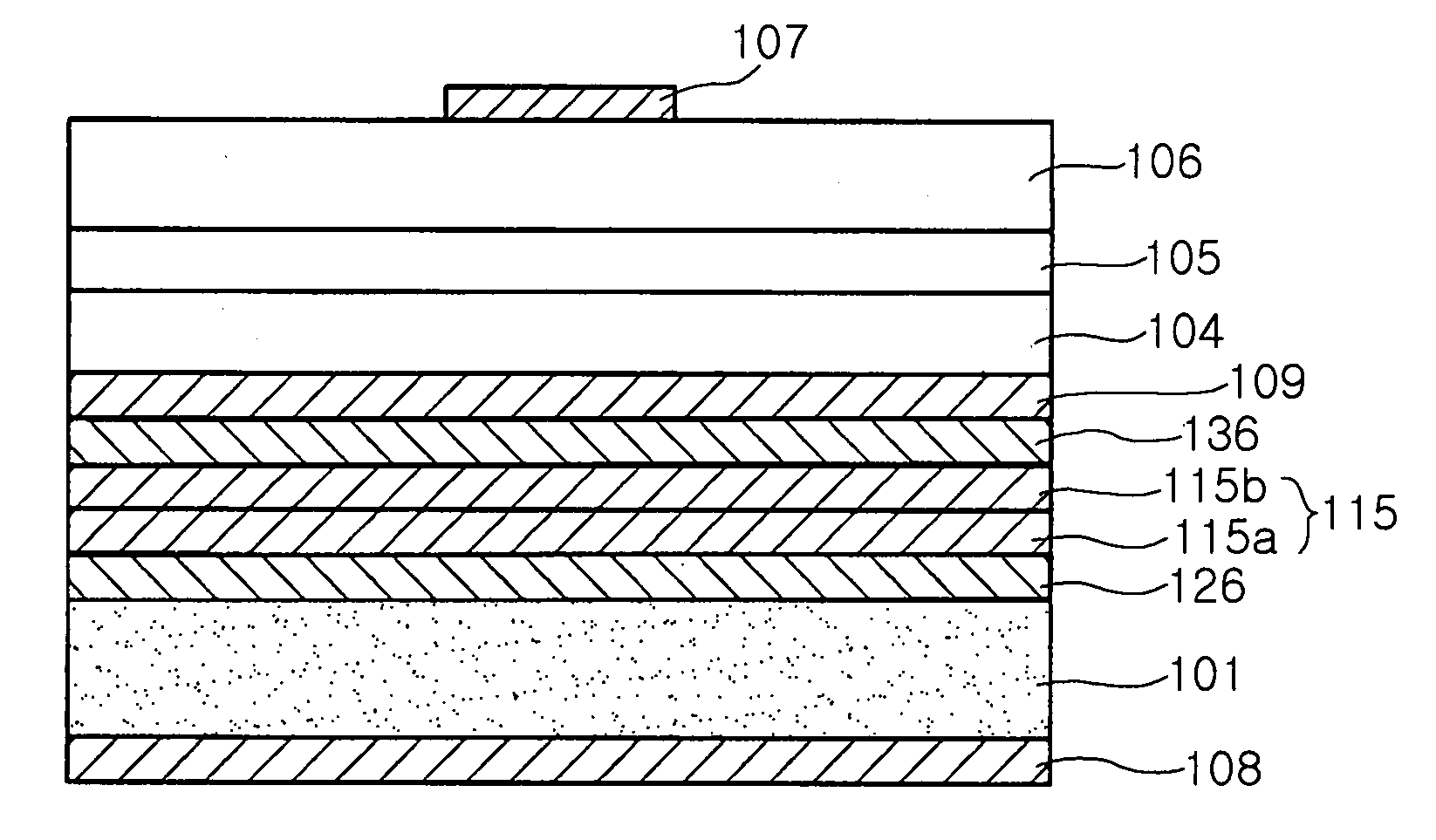
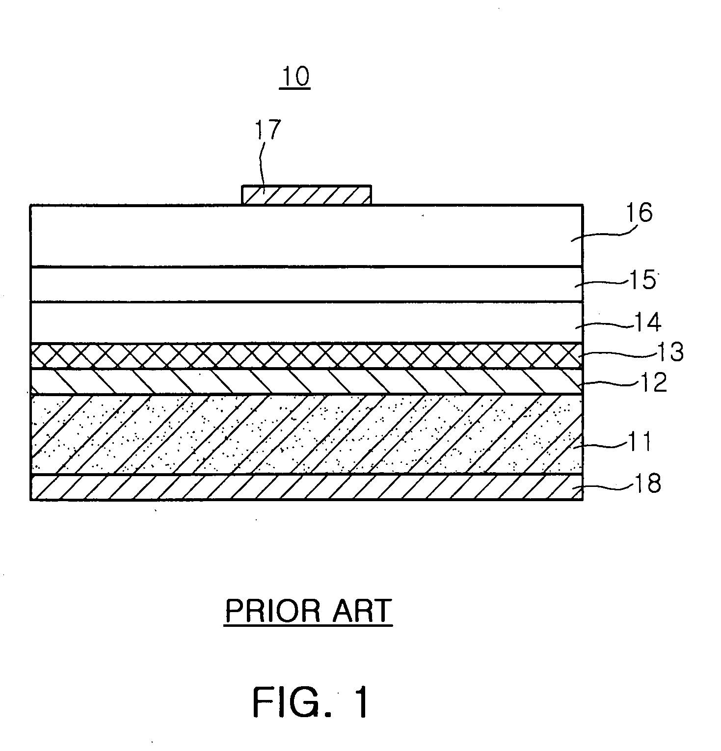
[0031]FIG. 3 is across-sectional view illustrating a vertical structure light emitting diode (LED) device 100 according to an embodiment of the present invention. Referring to FIG. 3, the vertical structure semiconductor LED device 100 includes a conductive substrate 101, a metal bonding layer 115, a p-type semiconductor layer 104, an active layer 105, and an n-type semi...


PUM

PropertyMeasurementUnit
temperatureaaaaaaaaaa
melting pointaaaaaaaaaa

Abstract

A method of manufacturing a vertical structure light emitting diode device, the method including: sequentially forming a first conductivity type III-V group compound semiconductor layer, an active layer, and a second conductivity type III-V group compound semiconductor layer on a substrate for growth; bonding a conductive substrate to the second conductivity type III-V group compound semiconductor layer; removing the substrate for growth from the first conductivity type III-V group compound semiconductor layer; and forming an electrode on an exposed portion of the first conductive III-V group compound semiconductor layer due to the removing the substrate for growth, wherein the bonding a conductive substrate comprises partially heating a metal bonding layer by applying microwaves to a bonding interface while bringing the metal bonding layer into contact with the bonding interface.

Description

CROSS-REFERENCE TO RELATED APPLICATIONS[0001]This application claims the priorities of Korean Patent Application Nos. 2006-0125015 and 2007-97025 filed on Dec. 8, 2006 and Sep. 21, 2007 respectively, in the Korean Intellectual Property Office, the disclosure of which is incorporated herein by reference.BACKGROUND OF THE INVENTION[0002]1. Field of the Invention[0003]The present invention relates to a vertical structure III-V group compound semiconductor light emitting diode (LED) device and a method of manufacturing the same, and more particularly, to a vertical structure semiconductor LED device capable of enabling wafer bonding at a low temperature and preventing occurrence of stress and a method of manufacturing the same.[0004]2. Description of the Related Art[0005]In general, III-V group GaN semiconductors shown as AlxGayIn(1-x-y)N (0≦x≦1, 0≦y≦1, and 0≦x+y≦1) are compound semiconductor materials suitable for emitting light in ranges of blue and ultraviolet and used for light emit...

Claims


Application Information

Patent Timeline
Patent Type & Authority Applications(United States)
IPC IPC(8): H01L33/00H01L33/32H01L33/40
CPCH01L33/0079H01L33/0093
Inventor CHO, MYONG SOOPARK, KI YEOLSONG, SANG YEOBLEE, SI HYUKCHOI, PUN JAE
Owner SAMSUNG ELECTRONICS CO LTD
Why Eureka
Try Eureka