Functional device and production method therefor

a technology of functional devices and production methods, applied in the direction of semiconductor devices, electrical apparatus, layered products, etc., can solve the problems of deteriorating photoelectric conversion efficiency, low doping efficiency, peeling from the interface, etc., to prevent cracks and peeling in the dielectric layer 32, high yield, excellent characteristics

Inactive Publication Date: 2004-08-12
SONY CORP
View PDF28 Cites 10 Cited by
  • Summary
  • Abstract
  • Description
  • Claims
  • Application Information

AI Technical Summary

Benefits of technology

0066] After that, for example, the not-illustrated oxide layer is heated with a laser beam emitted from a side close to the upper electrode 33 in a nitrogen gas atmosphere so as to be crystallized, thereby forming the dielectric layer 32. The parameters of the laser beam are similar to those in the first embodiment. In the third embodiment as well, as described in the first embodiment, heat transmission to the substrate 11 is suppressed by the inorganic heat resistant layer 13, a stress generated by the thermal expansion of the substrate 11 is shut off by the organic polymer layer 12, and occurrence of a crack and peeling in the dielectric layer 32 is prevented.
0067] As described above, in the embodiment as well, the organic polymer layer 12 is formed between the substrate 11 and the dielectric layer 32. Consequently, in a manner similar to the first embodiment, the occurrence of a crack and peeling in the dielectric layer 32 can be prevented, and the excellent dielectric film 32 can be formed on the substrate 11 made of the organic material at high yield. Thus, the light and shock-resistant dielectric capacitor 30 having excellent characteristics can be obtained.

Problems solved by technology

In the case of a solar battery, there are drawbacks such that doping efficiency is lower as compared with the case of using polysilicon, and photoelectric conversion efficiency deteriorates due to an increase in series resistance.
However, even small deformation of the substrate 101 causes a crack in the inorganic heat resistant layer 102 on the substrate 101, and peeling occurs from the interface.
In the case of manufacturing a functional device by using the organic material substrate, therefore, sufficient characteristics and reliability cannot be obtained.

Method used


Image

  • Functional device and production method therefor
  • Functional device and production method therefor
  • Functional device and production method therefor

Examples


example 2

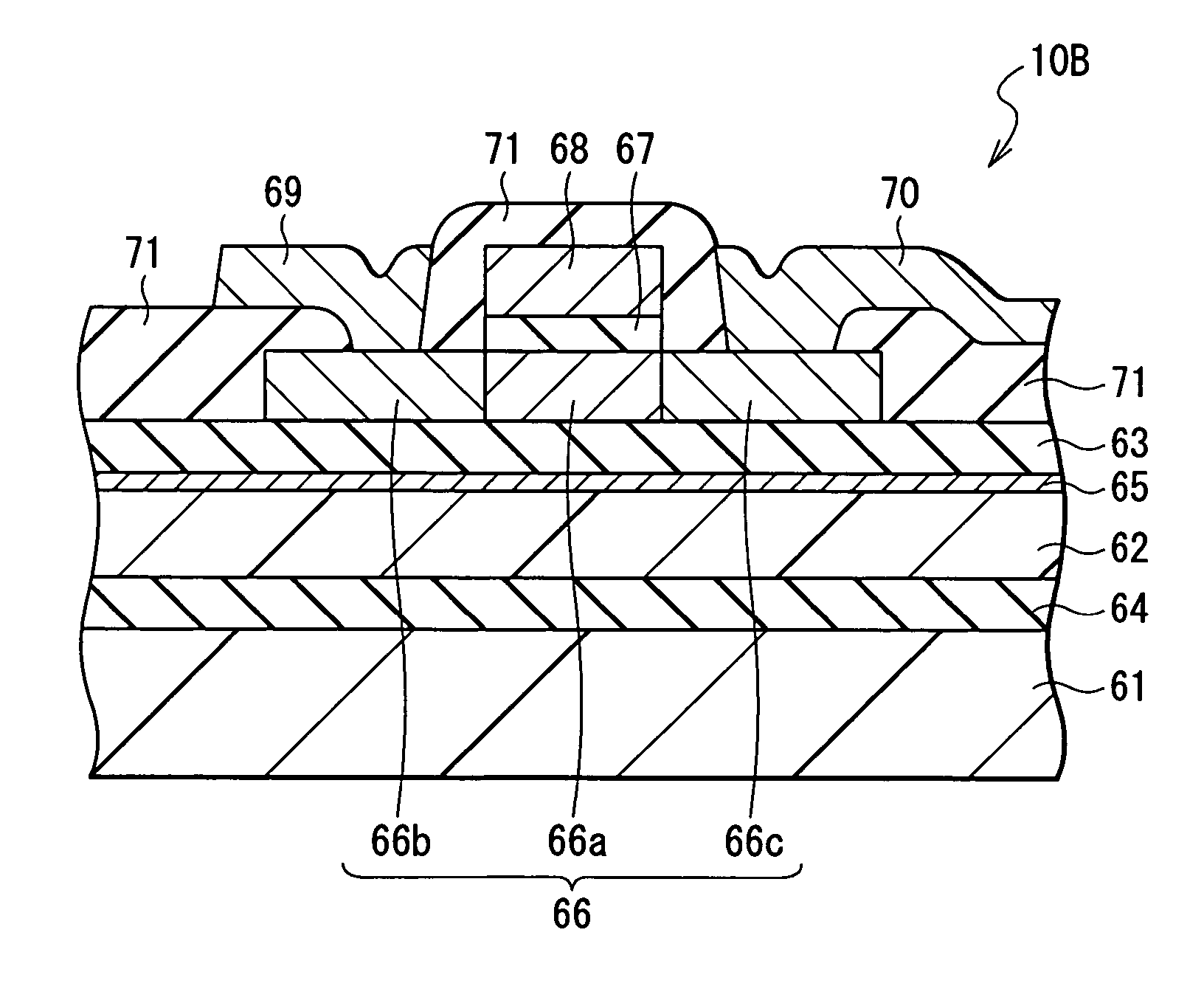
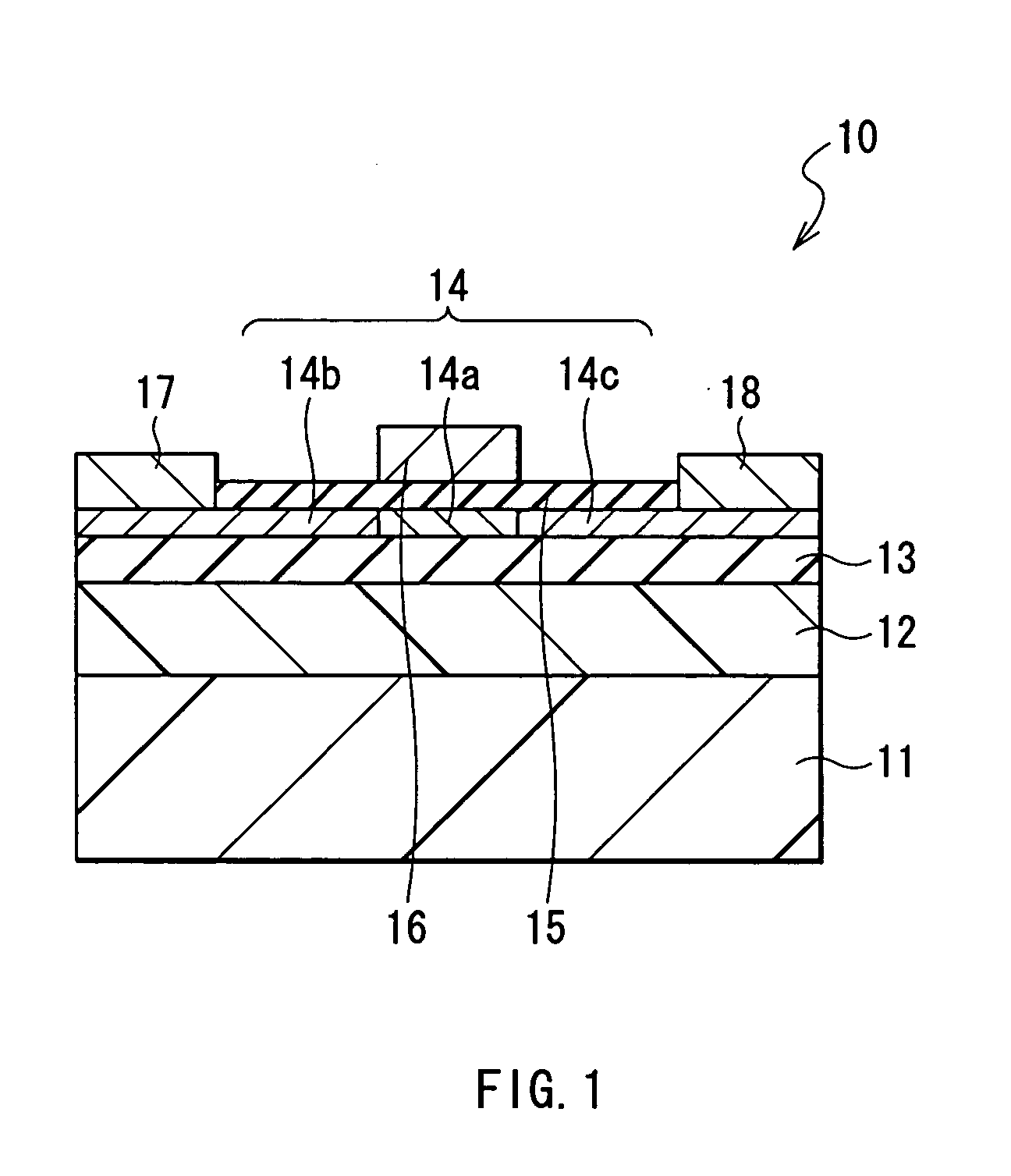
[0093] In this example, a polysilicon layer was formed in a manner similar to Example 1 except that an electrode made of ITO was formed between the inorganic heat resistant layer and the amorphous silicon layer. The polysilicon layer was also observed in a manner similar to Example 1. No crack and peeling was seen in the polysilicon layer and an excellent crystal layer was formed.

example 3

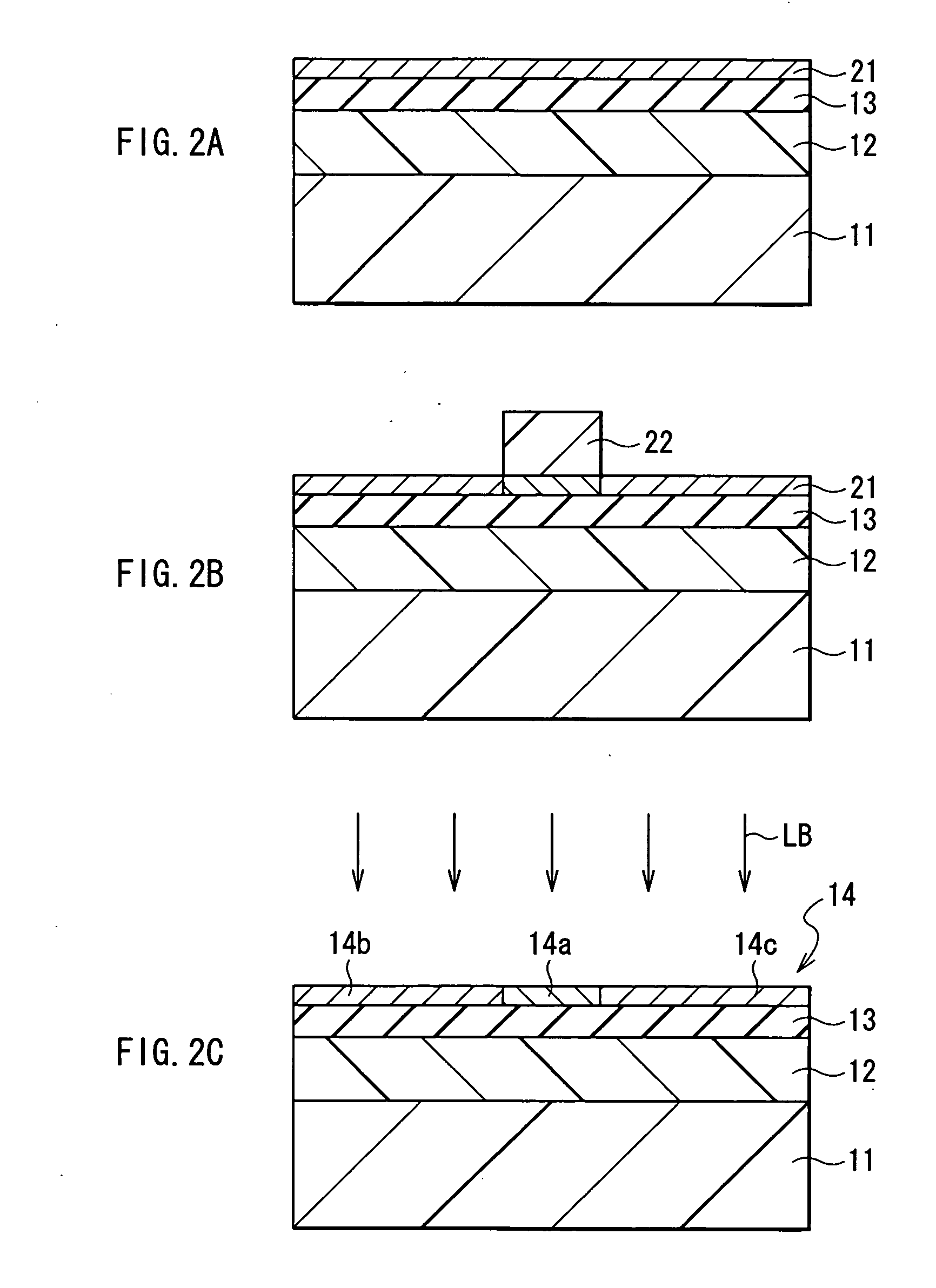
[0094] In this example, a polysilicon layer was formed in a manner similar to Example 1 except that after forming the amorphous silicon layer, prior to irradiation of a laser beam, phosphorus was doped at a high density into the amorphous silicon layer. After carrying the substrate into a PECVD (Plasma Enhanced Chemical Vapor Deposition) chamber by using a load lock, the phosphorus was doped by exposing the amorphous silicon layer to a plasma while passing a mixture gas of phosphine gas and hydrogen gas (Hs) containing 1% by volume of phosphine gas. The polysilicon layer was also observed in a manner similar to Example 1 and no cracks and peeling were found. It was understood that the excellent n+ type polysilicon layer can be formed on the substrate made of an organic material.

example 4

[0095] In this example, a polysilicon layer was formed in a manner similar to Example 1 except that, after forming the amorphous silicon layer, boron was doped at high density into the amorphous silicon layer prior to irradiation of a laser beam. Boron was doped in a manner similar to Example 3 except that a diborane gas was used in place of a phosphine gas. The polysilicon layer was also observed in a manner similar to Example 1 and no cracks and peeling were seen. That is, it was understood that the excellent p.sup.+ type polysilicon layer can be formed on the substrate made of an organic material.


PUM

PropertyMeasurementUnit
thicknessaaaaaaaaaa
thicknessaaaaaaaaaa
thicknessaaaaaaaaaa

Abstract

The invention provides a functional device having no cracks and capable of delivering good functional characteristics and a method of manufacturing the same. A functional layer (14) is formed by crystallizing an amorphous silicon layer as a precursor layer by laser beam irradiation. A laser beam irradiation conducts heat up to a substrate (11) to cause it to try to expand; a stress to be produced by the difference in thermal expansion coefficient between the substrate (11) and the functional layer (14) is shut off by an organic polymer layer (12) lower in thermal expansion coefficient than the substrate (ii), thereby causing no cracks nor separations in the functional layer (14). The organic polymer layer (12) is preferably made of an acrylic resin, an epoxy resin, or a polymer material containing these that is deformed by an optical or thermal process to undergo a three-dimensional condensation polymerization, for higher compactness and hardness. Inserting a metal layer and an inorganic heat resistant layer between the substrate (11) and the functional layer (14) will permit a more powerful laser irradiation.

Description

[0001] The present invention relates to a functional device having a functional layer, such as a thin film transistor, a dielectric capacitor, or a solar battery, and a method of manufacturing the same.[0002] Since the pn junction of a hydrogenated amorphous silicon was developed in 1976, the hydrogenated amorphous silicon has been being actively studied. The hydrogenated amorphous silicon has a structure in which a dangling bond in a network made of silicon is terminated by hydrogen or fluorine, and its film can be formed at a low temperature equal to or lower than 300.degree. C. Consequently, the film can be formed on a cheap glass substrate. A study is being made to apply the hydrogenated amorphous silicon to a functional device such as a thin film transistor (TFT), a solar battery, or an optical sensor.[0003] However, when the hydrogenated amorphous silicon is used as it is, in the case of a TFT, only carrier mobility as low as about 0.1 to 0.5 cm.sup.2 / V*S can be obtained. In t...

Claims


Application Information

Patent Timeline
Patent Type & Authority Applications(United States)
IPC IPC(8): B32B7/02H01L21/20H01L21/268H01L21/336H01L21/822H01L27/04H01L29/786H01L31/04
CPCH01L21/2026H01L21/268H01L29/66757H01L29/78678H01L29/78603H01L29/78675H01L29/66765H01L21/02532H01L21/02686H01L29/78
Inventor MACHIDA, AKIOGOSAIN, DHARAM PALUSUI, SETSUO
Owner SONY CORP
Why Eureka
Try Eureka