

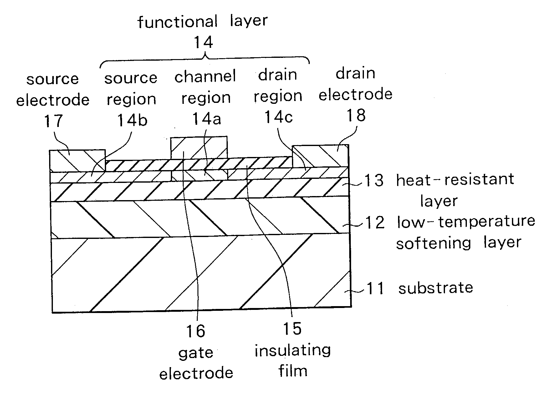
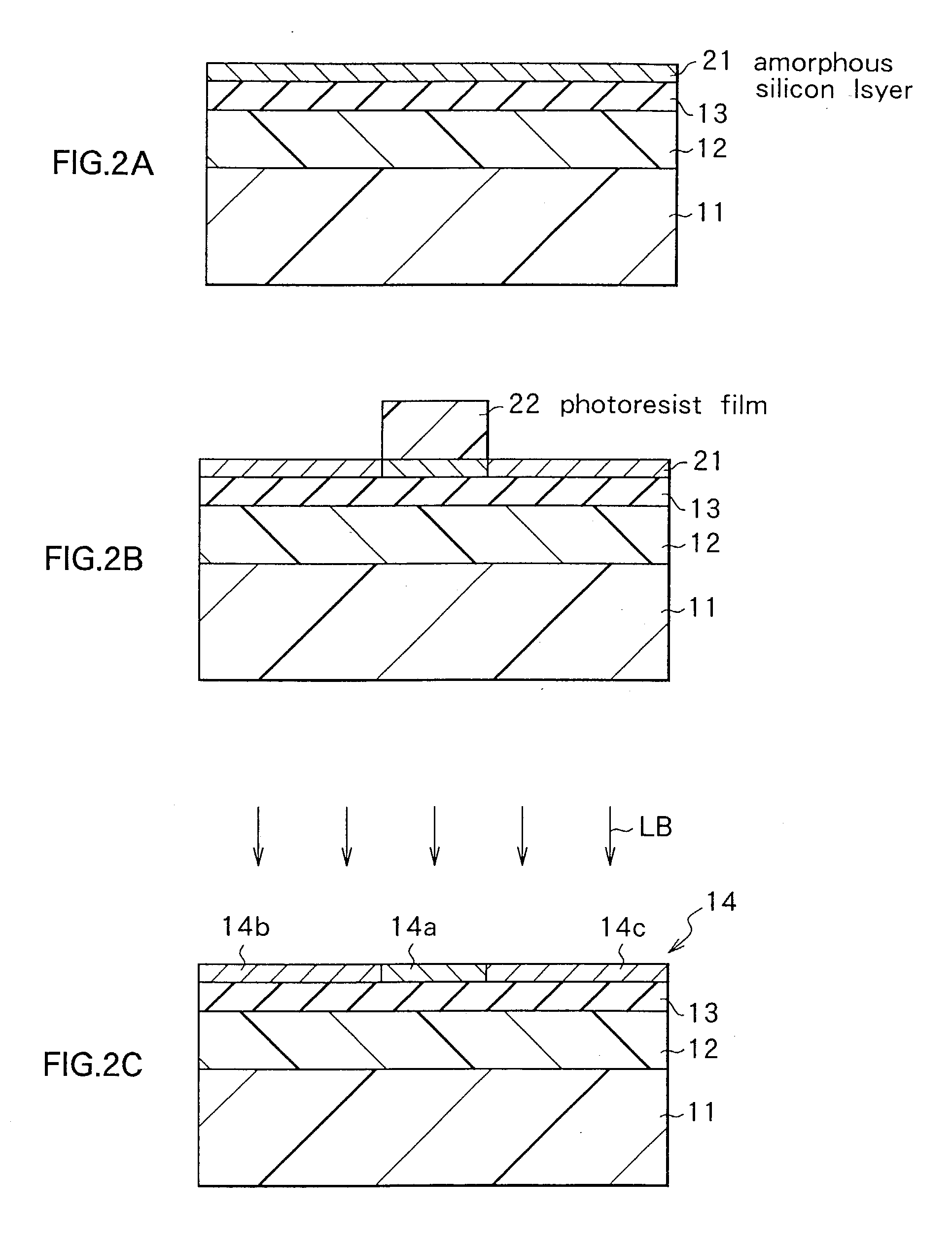
Functional device and method of manufacturing the same
a technology of functional devices and manufacturing methods, applied in the direction of bulk negative resistance effect devices, semiconductor devices, electrical devices, etc., can solve the problems of deteriorating photoelectric conversion efficiency, inability to obtain sufficient characteristics and reliability, and low doping efficiency, so as to prevent cracking and peeling in the dielectric layer 32, high yield, and excellent characteristics
- Summary
- Abstract
- Description
- Claims
- Application Information
AI Technical Summary
Benefits of technology
Problems solved by technology
Method used
Image

Examples
example 2
[0090] In this example, a polysilicon layer was formed in a manner similar to Example 1 except that an electrode made of aluminum was formed between the heat-resistant layer and the amorphous silicon layer. The polysilicon layer was also observed in a manner similar to Example 1. The result is shown in FIG. 11. No crack and peeling is seen in the polysilicon layer and an excellent crystal layer was formed.
[0091] As a comparative example of Example 2, a polysilicon layer was formed in a manner similar to Example 2 except that no low-temperature softening layer was formed. The polysilicon layer was also observed in a manner similar to Example 1. The result is shown in FIG. 12. A number of cracks are seen in the polysilicon layer and a part was completely peeled off.
[0092] It was understood that, even when an electrode is formed between the amorphous silicon layer and the heat-resistant layer, in a manner similar to Example 1, the excellent polysilicon layer could be formed on the subs...
example 3
[0093] In this example, the polysilicon layer was formed in a manner similar to Example 1 except that after forming the amorphous silicon layer, prior to irradiation of a laser beam, phosphorus was doped at a high density into the amorphous silicon layer. After carrying the substrate into a PECVD (Plasma Enhanced Chemical Vapor Deposition) chamber by using a load lock, the amorphous silicon layer was doped with phosphorus by exposing to plasma of a mixture gas of phosphine gas and hydrogen gas (Hs) containing 1% by volume of phosphine gas. The polysilicon layer was also observed in a manner similar to Example 1 and no cracks and peeling were found. It was understood that the excellent n-type polysilicon layer could be formed on the substrate made of an organic material.
example 4
[0094] In this example, a polysilicon layer was formed in a manner similar to Example 1 except that, after forming the amorphous silicon layer, boron was doped at high density into the amorphous silicon layer prior to irradiation of a laser beam. Boron was doped in a manner similar to Example 3 except that a diborane gas was used in place of a phosphine gas. The polysilicon layer was also observed in a manner similar to Example 1 and no crack and peeling was seen. That is, it was understood that the excellent p-type polysilicon layer could be formed on the substrate made of an organic material.
PUM
| Property | Measurement | Unit |
|---|---|---|
| softening temperature | aaaaa | aaaaa |
| temperature | aaaaa | aaaaa |
| carrier mobility | aaaaa | aaaaa |
Abstract
Description
Claims
Application Information