High light extraction efficiency light emitting diode (LED) with emitters within structured materials

a light emitting diode and high light extraction efficiency technology, applied in semiconductor/solid-state device manufacturing, electrical apparatus, semiconductor devices, etc., can solve the problems of weak interaction between structure's guided modes and crystals, high radiation emission rate, and difficult to achieve properties

Inactive Publication Date: 2008-06-12
RGT UNIV OF CALIFORNIA
View PDF17 Cites 59 Cited by
  • Summary
  • Abstract
  • Description
  • Claims
  • Application Information

AI Technical Summary

Problems solved by technology

However, such structures suffer from two drawbacks: (1) the radiative emission rate is highly suppressed, requiring (2) emitting species with very high radiative efficiency, a property not easily achievable at room temperature.
However, in such implementations, the interaction between the structure's guided modes and the crystal is rather weak, requiring a rather long photonic crystal, and consequently a large device, in order to extract most of the guided light.
First, possible diminished radiative efficiency due to the large free surface of the active region which is degraded when etching the photonic crystal structure. Nonetheless, high quality material can still be obtained, by using annealing steps following the etching, as described in [24]. Alternatively, high quality material can also be obtained by direct columnar growth of the structure.
Another problem results from the lower photonic density of states in the etched region, which is a natural consequence of the diminished average index of refraction.
Finally, another source of very diminished emission might be due to the emitting layer having a lower index than the surrounding layer, and thus not supporting guided or localized modes.

Method used


Image

  • High light extraction efficiency light emitting diode (LED) with emitters within structured materials
  • High light extraction efficiency light emitting diode (LED) with emitters within structured materials
  • High light extraction efficiency light emitting diode (LED) with emitters within structured materials

Examples


Embodiment Construction

[0062]In the following description of the preferred embodiment, reference is made to the accompanying drawings that form a part hereof, and in which is shown by way of illustration a specific embodiment in which the invention may be practiced. It is to be understood that other embodiments may be utilized and structural changes may be made without departing from the scope of the present invention.

[0063]Technical Description

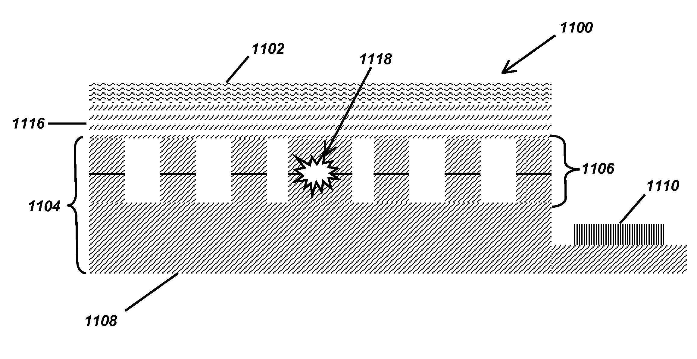
[0064]For conciseness throughout this disclosure, “(Al,Ga,In)N layer” will refer to an ensemble of layers deposited or grown by any technique, for example, by MBE (molecular beam epitaxy), MOCVD (metalorganic chemical vapour deposition) or VPE (vapour phase epitaxy), and usually comprising: a buffer layer grown on a substrate, one or more active layers such as quantum wells, quantum dots, barriers, or any other light emitting semiconductor layer, current blocking layers, contact layers, and other layers typically grown for a LED (light emitting diode) and well know...


PUM


Abstract

Light Emitting Diodes (LEDs) where the emission region, usually a (Al,In,Ga)N layer, is structured for efficient light extraction, are disclosed. The structuring is designed for light extraction from thin films, such as a photonic crystal acting as a diffraction grating. In addition, the structuring controls the in-plane emission and allows new modes into which light will be emitted. Various electrode designs are proposed, including ZnO structures which are known to lead to both excellent electrical properties, such as good carrier injection, and high transparency. Alternatively, the (Al,In,Ga)N layer can be replaced by structures with other materials compositions, in order to achieve efficient light extraction.

Description

CROSS-REFERENCE TO RELATED APPLICATIONS[0001]This application claims the benefit under 35 U.S.C. Section 119(e) of the following co-pending and commonly-assigned U.S. patent applications:[0002]U.S. Provisional Application Ser. No. 60 / 866,015, filed on Nov. 15, 2006, by Aurelien J. F. David, Claude C. A. Weisbuch, Steven P. DenBaars and Stacia Keller, entitled “HIGH LIGHT EXTRACTION EFFICIENCY LIGHT EMITTING DIODE (LED) WITH EMITTERS WITHIN STRUCTURED MATERIALS,” attorneys' docket number 30794.197-US-P1 (2007-113-1);[0003]which application is incorporated by reference herein.[0004]This application is related to the following co-pending and commonly-assigned applications:[0005]U.S. Utility application Ser. No. 10 / 581,940, filed on Jun. 7, 2006, by Tetsuo Fujii, Yan Gao, Evelyn. L. Hu, and Shuji Nakamura, entitled “HIGHLY EFFICIENT GALLIUM NITRIDE BASED LIGHT EMITTING DIODES VIA SURFACE ROUGHENING,” attorney's docket number 30794.108-US-WO (2004-063), which application claims the benef...

Claims


Application Information

Patent Timeline
Patent Type & Authority Applications(United States)
IPC IPC(8): H01L33/00H01L21/00H01L33/08H01L33/24H01L33/40H01L33/46
CPCH01L33/0079H01L33/08H01L2933/0083H01L33/405H01L33/46H01L33/24H01L33/0093
Inventor DAVID, AURELIEN J. F.WEISBUCH, CLAUDE C. A.DENBAARS, STEVEN P.KELLER, STACIA
Owner RGT UNIV OF CALIFORNIA
Why Eureka
Try Eureka