
Semiconductor Device

Active Publication Date: 2008-06-12
ROHM CO LTD
View PDF5 Cites 2 Cited by
  • Summary
  • Abstract
  • Description
  • Claims
  • Application Information

AI Technical Summary

Benefits of technology

[0004]In the both cases, however, the P-type diffusion region or the trench gate structure narrows the forward current path, resulting in a higher on-resistance and higher forward voltage (VF).
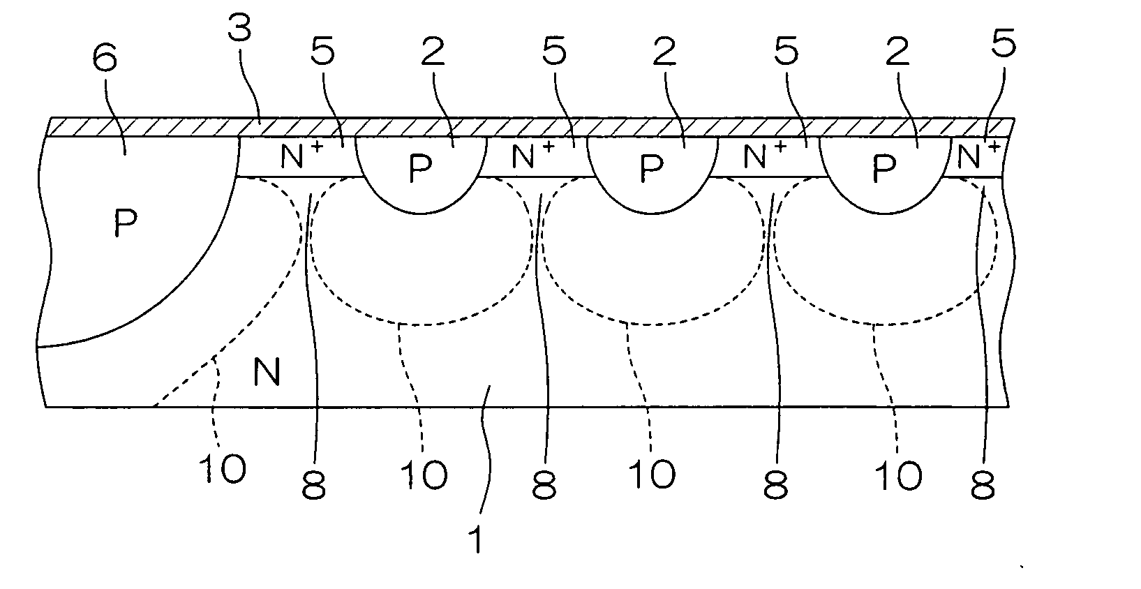
[0007]With this configuration, the leakage suppression structure can suppress or prevent the flow of reverse leakage current, and further, the highly doped layer can reduce the resistance in the forward current path, thereby reducing the on-resistance and the forward voltage (VF) that induces the forward current. Accordingly, the mutually contradictory requests on a Schottky barrier device can be satisfied at the same time.
[0008]It is preferable that the leakage suppression structure is formed across a region from a surface of the semiconductor substrate to a portion that is deeper than the highly doped layer, and includes an impurity diffusion layer of a second conductive type that is different from the first conductive type. With this configuration, when the reverse bias voltage is applied, the depletion layer that spreads from the impurity diffusion layer can without fail narrow or block the current path that flows across the highly impurity diffusion layer, thereby effectively achieving the reduction of the on-resistance through the highly impurity diffusion layer and the suppression of the reverse leakage current through the leakage suppression structure at the same time.
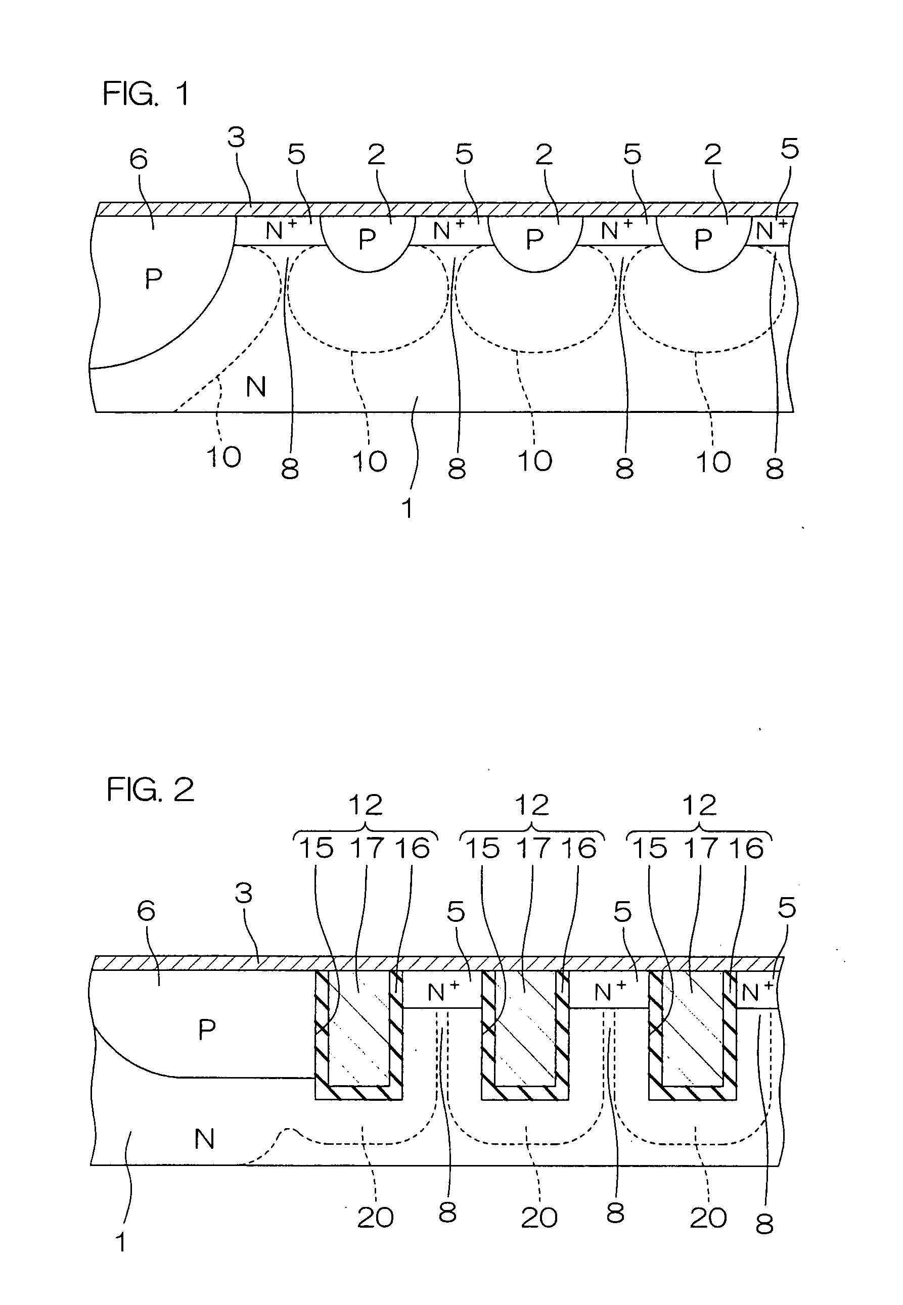
[0009]The leakage suppression structure may be formed across a region from a surface of the semiconductor substrate to a portion that is deeper than the highly doped layer, and includes a trench gate structure which is embedded with a gate electrode that is electrically connected to the Schottky electrode. With this configuration, when the reverse bias voltage is applied, the depletion layer that spreads from the trench gate structure can without fail narrow or block the current path that flows across the highly doped layer, thereby effectively achieving the reduction of the on-resistance through the highly doped layer and the suppression of the reverse leakage current through the leakage suppression structure at the same time.
[0010]Furthermore, it is preferable that the leakage suppression structure is designed to form a depletion layer that narrows or blocks the path of the leakage current flowing through the Schottky electrode and the semiconductor substrate, upon application of reverse bias voltage between the Schottky electrode and the semiconductor substrate. This configuration allows the reduction of the reverse leakage current without fail.

Problems solved by technology

Schottky barrier diodes have major problems to be solved: to reduce forward voltage (VF) that is necessary to induce forward current between the Schottky electrode and the semiconductor substrate; and to reduce a reverse leakage current (IR) that leaks upon application of reverse bias voltage between the Schottky electrode and the semiconductor substrate.
Because there is a trade-off relationship between the forward voltage VF and the reverse leakage current IR, it is difficult to satisfy the requirement at the same time.

Method used


Image

  • Semiconductor Device
  • Semiconductor Device

Examples


first embodiment

[0015]FIG. 1 shows a schematic cross-sectional view illustrating a configuration of a semiconductor device according to the present invention. The semiconductor device having a Schottky barrier diode comprises a semiconductor substrate 1 including a N-type silicon substrate; a P-type diffusion layer 2 (impurity diffusion layer) formed spaced apart in the surface region of the semiconductor substrate 1; and a Schottky electrode 3 formed on the surface of the semiconductor substrate 1. The P-type diffusion layer 2 is exposed on the surface of the semiconductor substrate 1 and electrically connected to the Schottky electrode 3. The impurity concentration of the P-type diffusion layer 2 is 1.0×10¹⁵ to 1.0×10¹⁹ atoms / cm3, for example. FIG. 1 shows the P-type diffusion layer 2 that includes a plurality of diffusion layers formed in parallel with each other to make a striped pattern. Alternatively, the diffusion layer 2 may include a plurality of diffusion layers that are spaced apart with...

second embodiment

[0021]FIG. 2 shows a schematic cross-sectional view illustrating a configuration of Schottky barrier diode which is a semiconductor device according to the present invention. In FIG. 2, elements corresponding to those in above FIG. 1 are designated by the same reference numeral.

[0022]In this embodiment, instead of using the P-type diffusion layer 2 in the aforementioned first embodiment, a trench gate structure 12 is used. Further in this embodiment, a plurality of the trench gate structures 12 are provided on the semiconductor substrate 1 so that a striped pattern is made. However, a plurality of the trench gate structures 12 may be formed spaced apart with each other to make, for example, a dotted pattern on the principal surface of the semiconductor substrate 1 as viewed from above.

[0023]The trench gate structure 12 comprises: a trench 15 having a predetermined depth (0.5 to 3.0 μm, for example) pierced from the surface of the semiconductor substrate 1, and having a rectangular c...


PUM


Abstract

The semiconductor device includes a first conductive type semiconductor substrate; a Schottky electrode forming a Schottky interface between a surface of the semiconductor substrate and itself; a leakage suppression structure, formed in a surface region of the semiconductor substrate, for suppressing a leakage current by generating a depletion layer when a reverse bias voltage is applied between the Schottky electrode and the semiconductor substrate; and a highly doped layer formed in the surface region of the semiconductor substrate in a region between the surface and the leakage suppression structure, the highly doped layer being the first conductive type, exhibiting a higher impurity concentration than the semiconductor substrate, and forming the Schottky interface between the Schottky electrode and itself.

Description

TECHNICAL FIELD[0001]The present invention relates to a semiconductor device comprising a Schottky electrode that Schottky-contacts with a semiconductor substrate.RELATED ART[0002]A Schottky barrier diode includes a semiconductor substrate and a Schottky electrode that has a Schottky junction with the surface of the semiconductor substrate. Schottky barrier diodes have major problems to be solved: to reduce forward voltage (VF) that is necessary to induce forward current between the Schottky electrode and the semiconductor substrate; and to reduce a reverse leakage current (IR) that leaks upon application of reverse bias voltage between the Schottky electrode and the semiconductor substrate. Because there is a trade-off relationship between the forward voltage VF and the reverse leakage current IR, it is difficult to satisfy the requirement at the same time.[0003]For example, Patent Document 1 discloses a Schottky barrier diode having a P-type diffusion region formed on the surface ...

Claims


Application Information

Patent Timeline
IPC IPC(8): H01L29/872
CPCH01L29/407H01L29/872H01L29/47
Inventor YOSHIMOCHI, KENICHI
Owner ROHM CO LTD
Learn More