Nitride semiconductor element and method for manufacturing same

A technology of nitride semiconductors and manufacturing methods, applied in semiconductor/solid-state device manufacturing, semiconductor devices, electrical components, etc., can solve the problems of Mg diffusion, reduced luminous efficiency, and increased man-hours, and achieve reduced impurity diffusion and high-efficiency luminescence , the effect of low forward voltage

Inactive Publication Date: 2012-02-01
PANASONIC CORP
View PDF2 Cites 0 Cited by
  • Summary
  • Abstract
  • Description
  • Claims
  • Application Information

AI Technical Summary

Problems solved by technology

In addition, if annealing is required, man-hours increase and manufacturing cost increases
Moreover, there is a problem that the added Mg diffuses into the light-emitting layer
If Mg is diffused, crystal defects will occur in the light-emitting layer, resulting in a decrease in internal quantum efficiency, and a significant decrease in luminous efficiency
On the other hand, as another example of the above-mentioned light-emitting element, as described in Non-Patent Document 1 and Non-Patent Document 2, a GaN layer having a (1-101) plane different from a C plane (0001) as a growth plane is added with In the case of carbon (C) co-growth, although a low-resistance p-type layer can be obtained, the growth conditions on the C-plane (0001) cannot be used, and currently it is necessary to use a 7°-inclined Si (001) plane. Substrates with uneven processing, such as inclined substrates, require more man-hours and higher manufacturing costs

Method used


Image

  • Nitride semiconductor element and method for manufacturing same
  • Nitride semiconductor element and method for manufacturing same
  • Nitride semiconductor element and method for manufacturing same

Examples


Embodiment approach 1

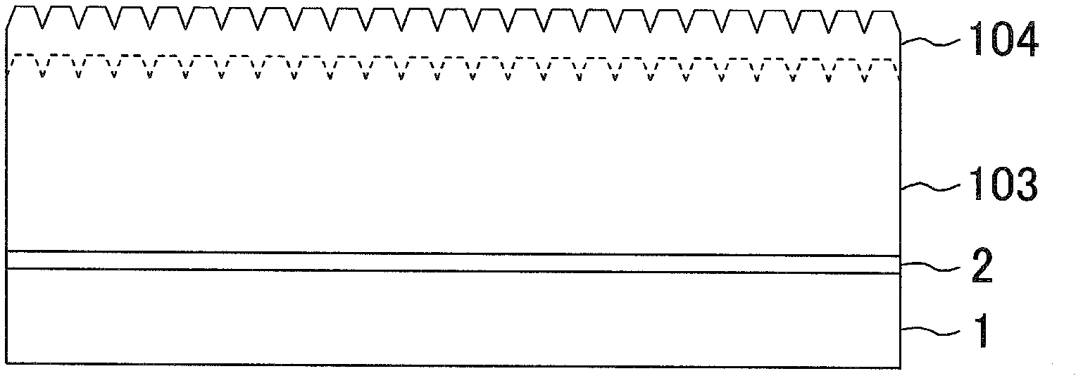
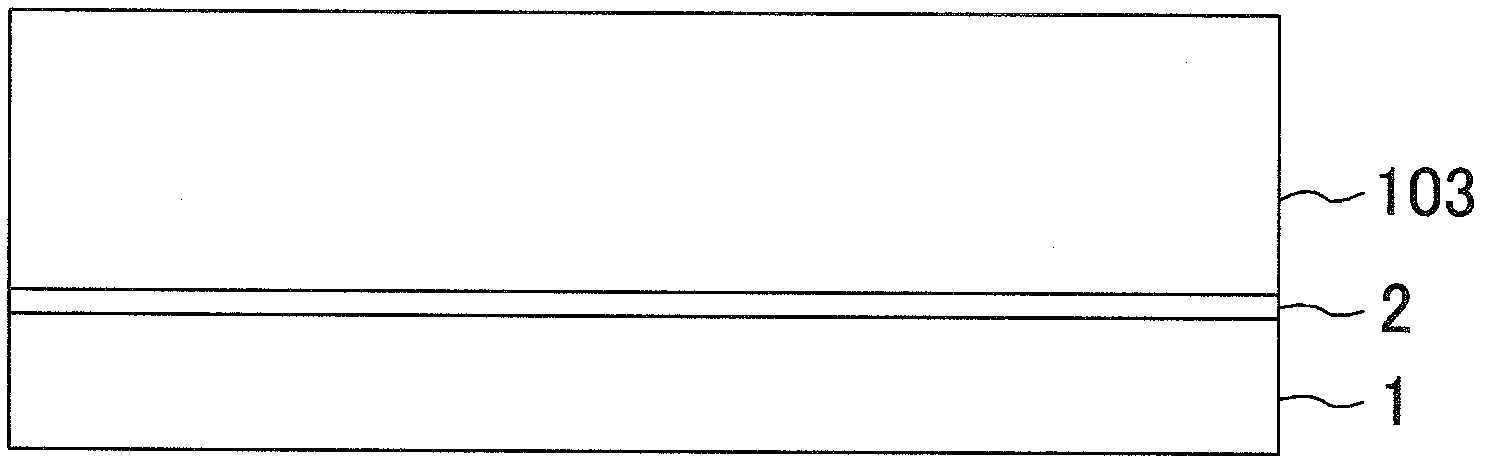
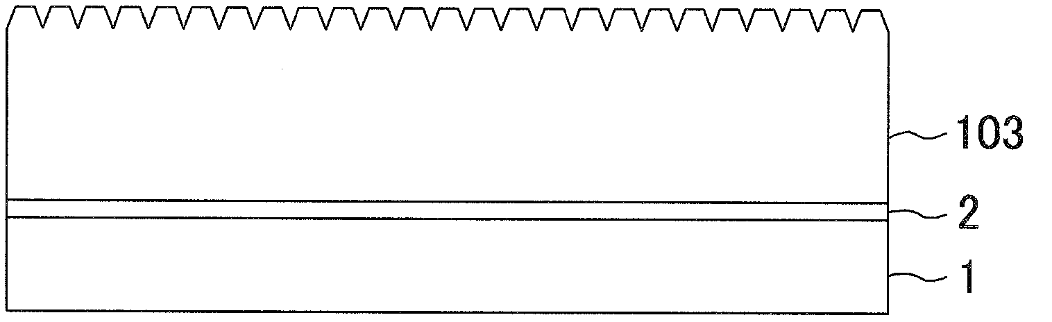
[0065] The first embodiment of the present invention will be described. figure 1 It is a cross-sectional view of the semiconductor laminated structure according to the first embodiment of the present invention.

[0066] In the semiconductor laminated structure of the first embodiment, on the Si substrate 1 with the (111) plane as the main surface, the buffer layer 2 made of AlN and the non-doped GaN are sequentially formed with the C plane (0001) plane as the growth plane. In the first nitride semiconductor layer 103 formed, a second nitride semiconductor layer 104 made of p-type GaN is formed on the first nitride semiconductor layer.

[0067] Here, the first nitride semiconductor layer 103 has unevenness, and the second nitride semiconductor layer 104 is formed in contact with the unevenness. At least a part of the uneven side surface of the first nitride semiconductor layer 103 is composed of a nitrogen polar surface, for example, (1-101). Carbon (C) is added to the second nitri...

Embodiment approach 2

[0083] Hereinafter, the second embodiment of the present invention will be described. image 3 It is a cross-sectional view of the LED according to the second embodiment of the present invention.

[0084] In the nitride semiconductor light-emitting element of the second embodiment, on the Si substrate 1 with the (111) plane as the main surface, the buffer layer 2 made of AlN and the n-type An n-type nitride semiconductor layer 3 made of GaN, a light emitting layer 4, an overflow suppression layer made of p-type AlGaN (hereinafter referred to as OFS layer) 5, and a first p-type nitride semiconductor layer made of p-type GaN 6. A second p-type nitride semiconductor layer 7 made of p-type GaN is formed on the first p-type nitride semiconductor layer 6, and the light-emitting layer 4, OFS layer 5, first p-type nitride semiconductor layer 6, A negative electrode 8 is formed on a region where a part of the second p-type nitride semiconductor layer 7 is exposed to the n-type nitride sem...

Embodiment approach 3

[0117] The third embodiment will be described. In the second embodiment, an LED was described, but the p-type nitride semiconductor layer of the present invention can also be applied to LD. Figure 8 It is a cross-sectional view of a laser diode (hereinafter referred to as LD) according to Embodiment 3 of the present invention.

[0118] In the nitride semiconductor light-emitting element of the third embodiment, on a substrate 201 made of n-type GaN with the (0001) plane as the main surface, the n-type Al a Ga 1-a N (0≤aa Ga 1-a The first p-type nitride semiconductor layer 6 composed of N (0a Ga 1-a The second p-type nitride semiconductor layer 7 composed of N (0b Ga 1-b A multiple quantum well structure formed by a well layer composed of N (0a Ga 1-a A current constriction layer 214 composed of N (0≤a<1). As a result, current can be selectively flowed through the current opening 215, and the light-emitting region can be drawn.

[0119] Here, the first p-type nitride semiconductor ...


PUM


Abstract

Disclosed is a nitride semiconductor element which comprises a first nitride semiconductor layer (103) wherein a growth surface is in the c plane and the upper surface is provided with recesses and projections, and a second nitride semiconductor layer (104) which is of p-type and formed on the first nitride semiconductor layer (103) so as to be in contact with the recesses and projections. The second nitride semiconductor layer (104) positioned right above the lateral surfaces of the recesses and the projections has a p-type carrier concentration of not less than 1 1018 / cm3.

Description

Technical field [0001] The present invention relates to a p-type nitride semiconductor layer that can be applied to semiconductor elements such as light emitting diodes and semiconductor lasers and a method of manufacturing the same, and a nitride semiconductor element using the p-type nitride semiconductor layer and a method of manufacturing the same. Background technique [0002] The so-called nitride semiconductor composed of GaN, InN, AlN, and their mixed crystals (mix crystal) has a band gap corresponding to the wavelength region from the visible region to the ultraviolet region, and can be achieved in green or blue A material for high-output light-emitting diodes in the wavelength range from color to ultraviolet. It is a material system that has been applied to semiconductor lasers and high-brightness light-emitting diodes (Light Emitting Diode: LED) since the realization of p-type GaN on a sapphire substrate with high quality. [0003] The following technology is proposed: ...

Claims


Application Information

Patent Timeline
Patent Type & Authority Applications(China)
IPC IPC(8): H01L33/32H01L21/205H01L33/22
CPCH01L21/02458H01L21/0237H01L21/02494H01L21/0254H01L21/0243H01L33/22H01L21/0262H01L21/02579H01L21/02502H01L33/32H01L21/02433H01L21/02507H01L21/02381H01L21/02516
Inventor 福岛康之上田哲三
Owner PANASONIC CORP
Why Eureka
Try Eureka