

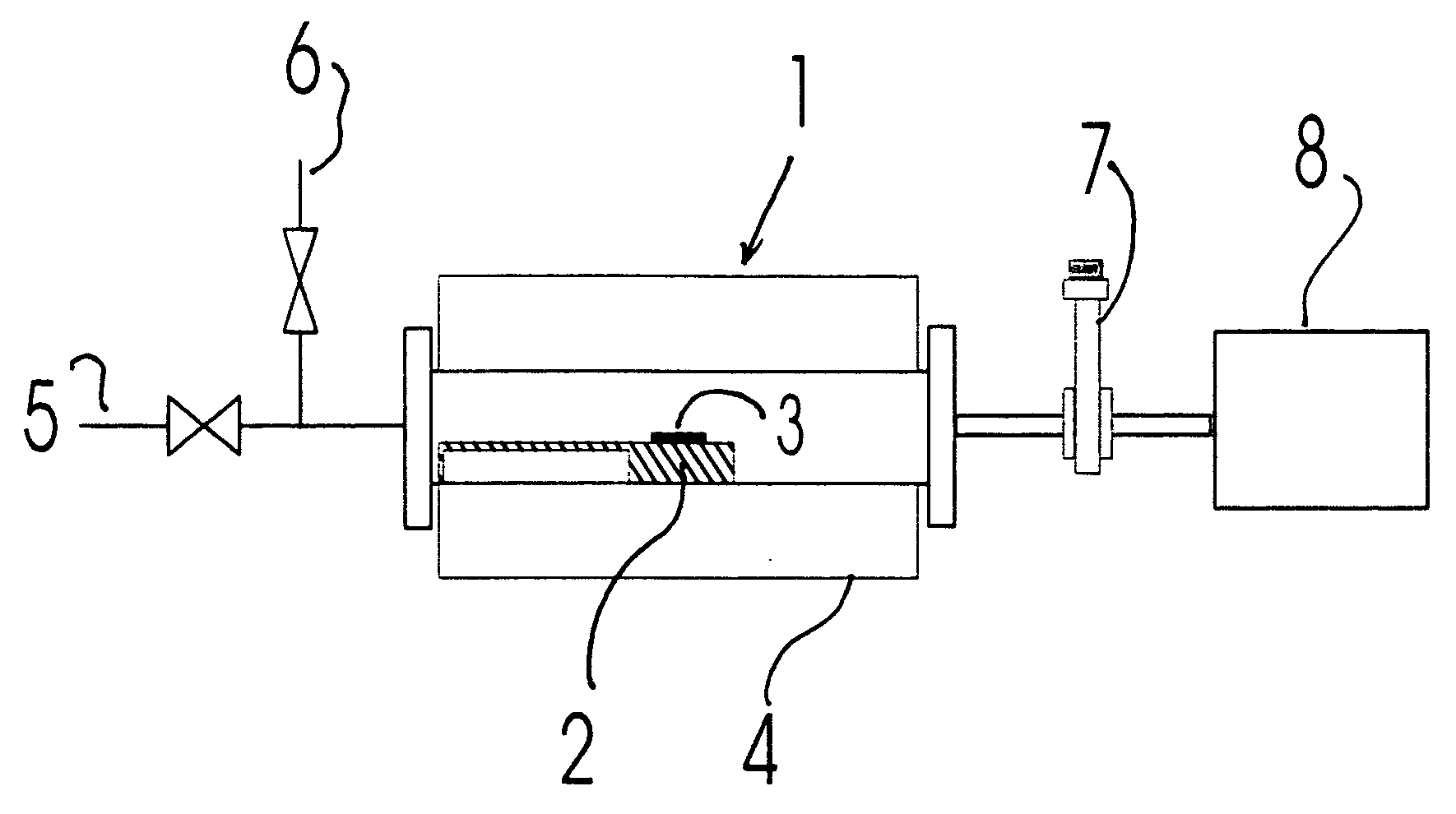
Thermal F2 etch process for cleaning CVD chambers
a technology of cvd chambers and etching processes, which is applied in the direction of chemistry apparatus and processes, lighting and heating apparatus, coatings, etc., can solve the problems of high particle contamination of device wafers from film spalling, and serious thermal budgets
- Summary
- Abstract
- Description
- Claims
- Application Information
AI Technical Summary
Benefits of technology
Problems solved by technology
Method used
Image

Examples
experiment i
[0013]In the first experiment, the reactor tube was maintained at 4000 C temperature and with 30 torr pressure. The different concentrations of pre-diluted F2 in N2 were introduced into the reactor tube. The results of thermal etch rate measurements for silicon nitride (SiNx) etched with pre-diluted F2 in N2 as a function of F2 concentration are given in Table I.
TABLE IEtch Rates for Silicon Nitride as a Function of F2 ConcentrationTemperaturePressureEtch Rate% F2 in N2(° C.)(torr)(nm / min)2.54003017540030292040030155
[0014]The results show that the dilute (no greater than 20%) molecular fluorine has a low thermal activation temperature. The F2 reacts with the silicon nitride to form SiF4 that can be pumped from the chamber. The etch rates are 17 nm / min for 2.5% F2, 29 nm / min for 5% F2 and 155 nm / min for 20% F2. The results show that the etch rate increases as the F2 concentration increases at the fixed temperature and pressure. The results further show that even at a very low concent...
experiment ii
[0015]To further determine the thermal etch rate of silicon nitride by pre-diluted 20% F2 in N2, a design of experiment (DOE) study was carried out. The parameter space of the DOE study covered a temperature range of 230° C. to 511° C. and a pressure range of 10 to 103 torr. A total of 12 silicon nitride etch rates were determined at various temperatures and pressures.
[0016]The results of thermal etch rate measurements for silicon nitride etched with pre-diluted 20% F2 at various temperatures and pressures are given in Table II. The results again show that the dilute (no greater than 20%) molecular fluorine has the low thermal activation temperature, etching of silicon nitride occurs even at a low temperature such as 2300 C.
TABLE IIEtch Rates for Silicon NitrideExperimentalTemperaturePressureEtch RateRun(° C.)(torr)(nm / min)123051.511.2223110117.6323410.36.6426210360.25374100236.9637855.8139.7740331290.9840430.5271.2940530.4205.910510100770.31151110629.21251151.8713.1
[0017]The data s...
experiment iii
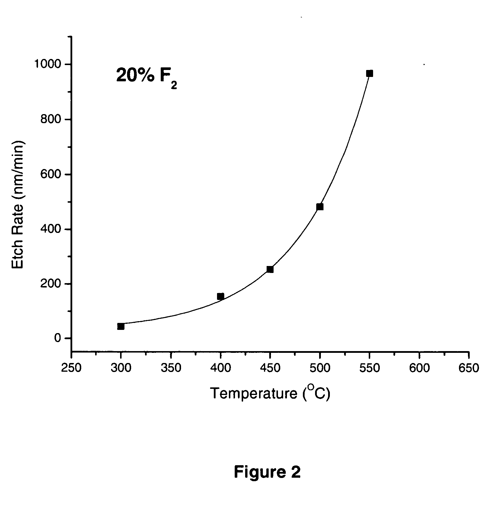
[0018]Based on the second experiment, the etch rate with pre-diluted 20% F2 at various temperatures with a fixed pressure was further investigated. In this experimental set, a series of thermal etch rate experiments were carried out with 20% F2 in N2 at 30 torr with temperatures ranging from 300° C. to 550° C. The experimental data of the etch rate versus temperature is plotted in FIG. 2.
[0019]The etch rates for 20% F2 are 53 nm / min at 3000 C, 139 nm / min at 4000 C, and increasing rapidly to 965 nm / min at 5500 C. The data shows that the etch rate increases exponentially as the temperature increases, as evidenced by the solid line of exponential fitting in FIG. 2.
[0020]FIG. 3 is a graph showing the thermal NF3 etch rate of silicon nitride films deposited with BTBAS by pre-diluted 20% NF3 in N2 as a function of temperatures ranging from 500° C. to 600° C. at 30 torr. The data is extracted from FIG. 1 in D. Foster, J. Ellenberger, R. B. Herring, A. D. Johnson, and C. L. Hartz, “In-situ ...
PUM
| Property | Measurement | Unit |
|---|---|---|
| Temperature | aaaaa | aaaaa |
| Temperature | aaaaa | aaaaa |
| Fraction | aaaaa | aaaaa |
Abstract
Description
Claims
Application Information