Bidirectional switch and method for driving bidirectional switch

a bidirectional switch and bidirectional switch technology, applied in the direction of electronic switching, diodes, pulse techniques, etc., can solve the problems of increasing cost, limiting the reduction of on-resistance, power loss due to on-effect,

Inactive Publication Date: 2008-06-19
PANASONIC CORP
View PDF16 Cites 54 Cited by
  • Summary
  • Abstract
  • Description
  • Claims
  • Application Information

AI Technical Summary

Benefits of technology

[0020]According to the second bidirectional switch driving method, the gate potential is fixed to the potential of the second reference electrode, and the potential of the second reference electrode is a floating potential. Therefore, a large forward bias which c

Problems solved by technology

As a result, when the switch is in the ON state, power loss occurs due to the ON-resistance of the diode in addition to power loss due to the ON-resistance of the IGBT or MOS FET.
Further, the increased number of elements causes an increase in cost.
Also, in a bidirectional switch which employs a conventional triac or the like, there is a l

Method used


Image

  • Bidirectional switch and method for driving bidirectional switch
  • Bidirectional switch and method for driving bidirectional switch
  • Bidirectional switch and method for driving bidirectional switch

Examples


first embodiment

Variation of First Embodiment

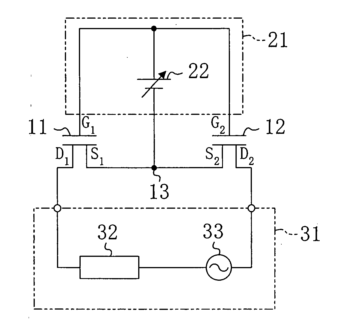
[0045]Hereinafter, a variation of the first embodiment will be described with reference to the drawings. FIG. 2 shows a circuit configuration of a bidirectional switch according to the variation of the first embodiment. In FIG. 2, the same parts as those of FIG. 1 are indicated by the same reference numerals and will not be described.

[0046]As shown in FIG. 2, in the bidirectional switch of this variation, the switch controller 21 is configured such that the control power supply 22 can be cut off from the circuit, and the node 13 and the gate terminal G1 and the gate terminal G2 can be short-circuited.

[0047]Specifically, the control power supply 22 is connected via a first switch 23A to the node 13, and via a second switch 23B to the gate terminal G1 and the gate terminal G2. The first switch 23A and the second switch 23B can be switched together so that the control power supply 22 can be cut off from the switch controller 21. The first switch 23A is a si...

second embodiment

Variation of Second Embodiment

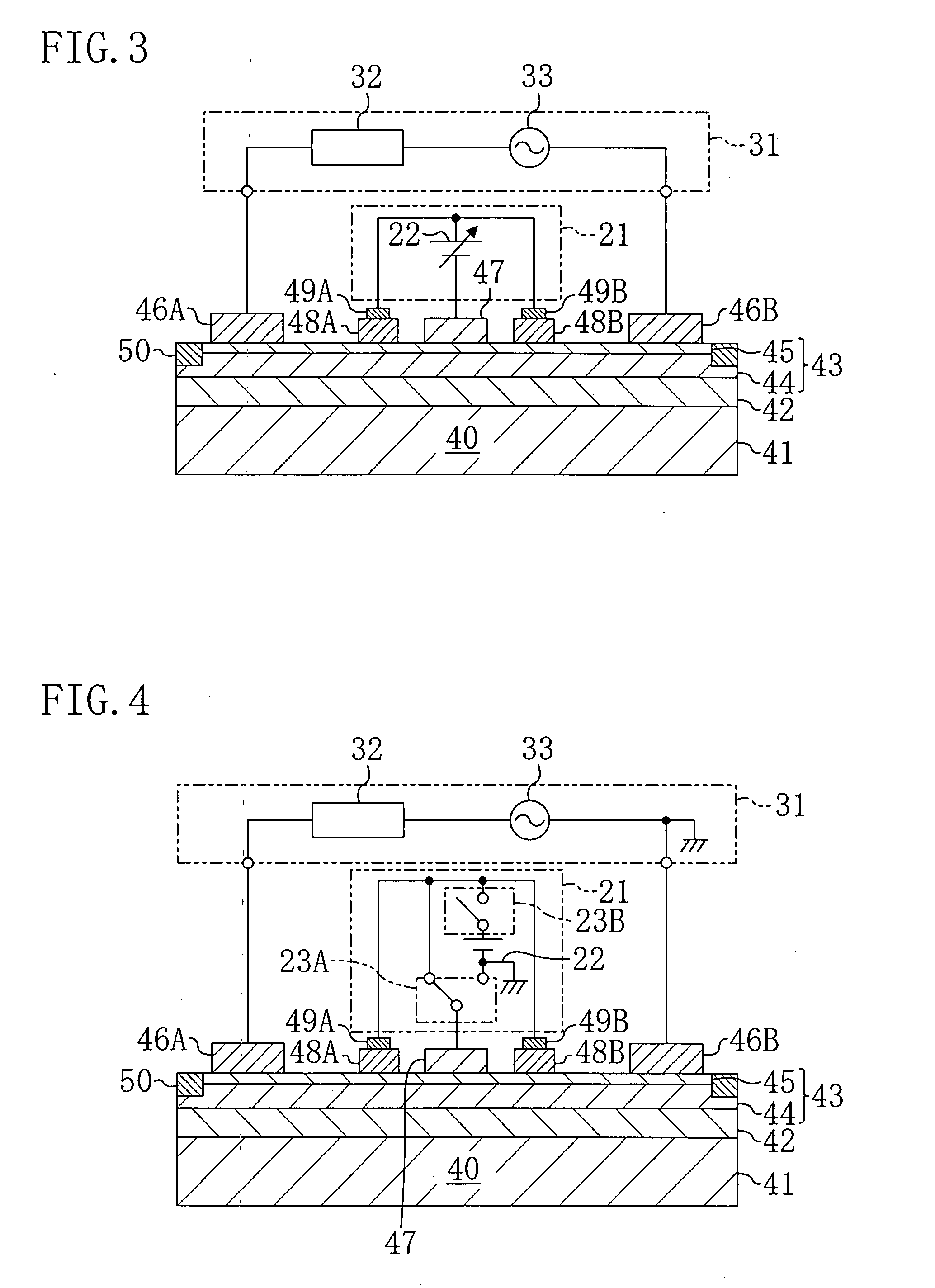
[0070]Hereinafter, a variation of the second embodiment will be described with reference to the drawings. FIG. 8 shows a configuration of a bidirectional switch according to the variation of the second embodiment. In FIG. 8, the same parts as those of FIG. 3 are indicated by the same reference numerals and will not be described.

[0071]The bidirectional switch of this variation has a first diode 61A connected between the first ohmic electrode 46A and the reference electrode 47 and a second diode 61B between the second ohmic electrode 46B and the reference electrode 47.

[0072]The first diode 61A and the second diode 61B are a free-wheel diode for preventing excessively large current from being applied to the bidirectional switching device 40 at the instant when the bidirectional switch is turned OFF (where the load 32 is an inductive load (L load)), thereby avoiding breakdown of the bidirectional switch.

[0073]The first diode 61A and the second diode 61B may...

third embodiment

[0078]Hereinafter, a third embodiment of the present invention will be described with reference to the drawings. FIG. 10 shows a configuration of a bidirectional switch according to the third embodiment.

[0079]As shown in FIG. 10, the bidirectional switch of this embodiment comprises a bidirectional switching device 70 and a switch controller 21. The bidirectional switching device 70 has a semiconductor layer 73 which is grown via a buffer layer 72 on a substrate 71 made of silicon (Si) or the like. The semiconductor layer 73 includes an undoped GaN layer 74 having a thickness of 2 μm and an undoped AlGaN layer 75 having a thickness of 25 nm, which are epitaxially grown in this order from below. In an interface region of the undoped GaN layer 44 with respect to the undoped AlGaN layer 45, a 2DEG layer which serves as a channel region is formed due to an influence of spontaneous polarization and piezoelectric polarization.

[0080]A first ohmic electrode 76A and a second ohmic electrode ...


PUM


Abstract

A bidirectional switch comprises a first FET, a second FET, and a switch controller for controlling a conductive state in which current from a bidirectional power supply electrically connected to drain terminals bidirectionally flows, and a nonconductive state in which the current does not flow. In the conductive state, the switch controller applies, to gate terminals of the first FET and the second FET, a voltage higher than a threshold voltage with reference to a potential at a node to which source terminals of the first FET and the second FET are connected. In the nonconductive state, the switch controller causes the bidirectional power supply and each gate terminal to be electrically insulated from each other, and applies a voltage lower than or equal to the threshold voltage with reference to the potential at the node.

Description

CROSS REFERENCE TO RELATED APPLICATIONS[0001]This Non-provisional application claims priority under 35 U.S.C. §119(a) on Patent Application No. 2006-336952 filed in Japan on Dec. 14, 2006, the entire contents of which are hereby incorporated by reference.BACKGROUND OF THE INVENTION[0002]1. Field of the Invention[0003]The present invention relates to a bidirectional switch having a low ON-resistance and a method for driving the bidirectional switch.[0004]2. Description of the Related Art[0005]There are known switching power semiconductor devices, such as a power MOS FET (Metal Oxide Film Semiconductor Field-Effect Transistor), an IGBT (Insulated Gate Bipolar Transistor), a thyristor, a triac, and the like. When these semiconductor devices are used to form a switching circuit capable of provide bidirectional current flow, the semiconductor devices need bidirectional high breakdown voltages.[0006]Power MOS FETs and IGBTs generally have a low reverse breakdown voltage. Therefore, a bidi...

Claims


Application Information

Patent Timeline
IPC IPC(8): H03K17/687
CPCH01L29/2003H01L29/7786H03K17/725H03K17/567H03K17/6874H03K17/063H01L27/085H01L29/1066H01L27/0629H01L27/0605H01L21/8252
Inventor YANAGIHARA, MANABUMORITA, TATSUOUEMOTO, YASUHIRO
Owner PANASONIC CORP
Why Eureka
Try Eureka