Display device, method of manufacturing display device, and electronic apparatus

a display device and display device technology, applied in the direction of optics, electrical devices, instruments, etc., can solve the problems of reducing the height presenting an obstacle to efforts to make the portable terminal low in profile, and no consideration for the mounting of the cog chip

Active Publication Date: 2008-06-19
JAPAN DISPLAY WEST
View PDF10 Cites 22 Cited by
  • Summary
  • Abstract
  • Description
  • Claims
  • Application Information

AI Technical Summary

Benefits of technology

[0031]According to further embodiment of the present invention, there is provided a method of manufacturing a display device having a first substrate with a pixel switch and drivers mounted thereon, a second substrate disposed in facing relation to the first substrate, and a material layer held between the first substrate and the second substrate and sealed by a seal member, including the steps of mounting a semiconductor chip having a control system for controlling the drivers, as a COG component on the first substrate parallel to a region in which the seal member and the second substrate are stacked, filling a space around the semiconductor chip with a protective fixing member thereby to secure the first substrate and the semiconductor chip to each other, and simultaneously polishing the second substrate and the semiconductor chip to the same thickness as each other.

Problems solved by technology

If a liquid crystal display device for use in a portable terminal display is thick, then it presents an obstacle to efforts to make the portable terminal low in profile.
According to Patent Document 1, however, since a TCP is used as an external terminal, no consideration for the mounting of a COG chip has been made.
If a COG chip is mounted on a TFT glass substrate, then the height of the COG chip is greater than the thickness of a facing glass substrate, making it difficult to reduce the thickness of the liquid crystal panel.
The disclosed liquid crystal panel is not suitable for making a liquid crystal display device compact.
Actually, however, the liquid crystal panel includes polarizing plate and phase difference plate combinations, and Patent Document 3 fails to show that the thickness of the COG chip is smaller than the total thickness including the thickness of the polarizing plate and phase difference plate combinations.
However, the thickness of the films may not be reduced to a minimum because the adhesive and the films need to have a certain level of mechanical strength.
Therefore, the proposal according to Patent Document 4 is not effective to manufacture desired low-profile liquid crystal panels.
According to Patent Document 5, the polishing process is complex and involves an increased number of steps.
As a result, though the structure proposed in Patent Document 5 is applicable to large-size liquid crystal displays as large as at least 6 inches, it may not be incorporated in smaller liquid crystal display modules because small-size, high-definition liquid crystal display devices as large as at most 6 inches require a polished area other than the pad area.

Method used


Image

  • Display device, method of manufacturing display device, and electronic apparatus
  • Display device, method of manufacturing display device, and electronic apparatus
  • Display device, method of manufacturing display device, and electronic apparatus

Examples


first embodiment

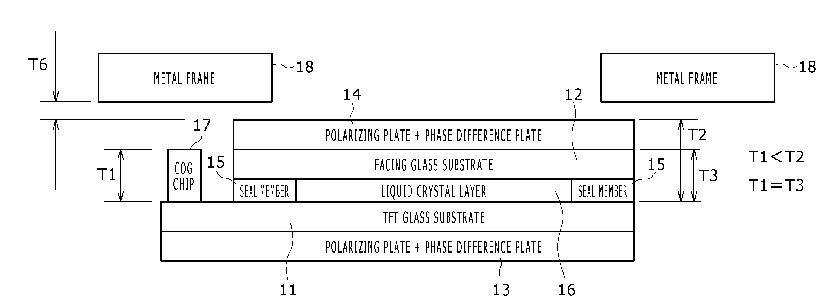
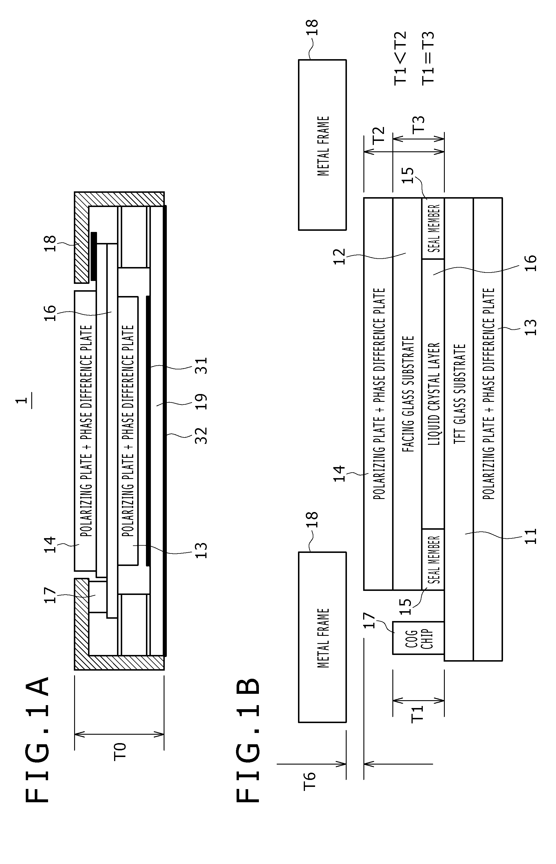
[0054]FIGS. 1A and 1B show in cross section a liquid crystal display device according to a first embodiment of the present invention. Specifically, FIG. 1A shows an overall cross-sectional structure of a liquid crystal panel of the liquid crystal display device according to the first embodiment, and FIG. 1B shows the cross-sectional structure in greater detail. According to the first embodiment, the liquid crystal panel has a liquid crystal layer as a material layer having an electrooptical effect.

[0055]As shown in FIGS. 1A and 1B, the liquid crystal display device, generally denoted by 1, includes a TFT (Thin Film Transistor) glass substrate 11 as a first transparent insulating substrate supporting thereon pixel switches and a driver circuit therefor which are constructed of TFTs, a facing glass substrate 12 as a second transparent insulating substrate disposed in facing relation to the TFT glass substrate 11, polarizing plate and phase difference plate combinations 13, 14 mounted ...

second embodiment

[0073]FIG. 5 shows in cross section a liquid crystal display device according to a second embodiment of the present invention.

[0074]As shown in FIG. 5, the liquid crystal display device, generally denoted by 2, includes: a TFT glass substrate 21 as a first transparent insulating substrate supporting thereon pixel switches and a driver circuit therefor which are constructed of TFTs; a facing glass substrate 22 as a second transparent insulating substrate disposed in facing relation to the TFT glass substrate 21; a liquid crystal layer 26 positioned between the TFT glass substrate 21 and the facing glass substrate 22 and having peripheral edges sealed by a seal member 25; polarizing plate and phase difference plate combinations 23, 24 disposed between the TFT glass substrate 21 and the liquid crystal layer 26 and between the liquid crystal layer 26 and the facing glass substrate 22; the liquid crystal layer 26 being held between the polarizing plate and phase difference plate combinat...


PUM

PropertyMeasurementUnit
total thickness T2aaaaaaaaaa
sizeaaaaaaaaaa
thickness T3aaaaaaaaaa

Abstract

Disclosed herein is a display device including: a first substrate with a pixel switch and drivers mounted thereon; a second substrate disposed in facing relation to the first substrate; a material layer held between the first substrate and the second substrate and having peripheral edges sealed by a seal member, the material layer having an electrooptical effect; and a semiconductor chip mounted as a COG component on the first substrate, the semiconductor chip having a control system configured to control the drivers; wherein the semiconductor chip having a thickness equal to the total thickness of the seal member and the second substrate or larger than the thickness of the seal member and smaller than the total thickness.

Description

CROSS REFERENCES TO RELATED APPLICATIONS[0001]The present invention contains subject matter related to Japanese Patent Application JP 2006-069539 filed in the Japan Patent Office on Mar. 14, 2006, the entire contents of which being incorporated herein by reference.BACKGROUND OF THE INVENTION[0002]1. Field of the Invention[0003]The present invention relates to a display device, a method of manufacturing such a display device, and an electronic apparatus for use in a portable terminal such as a cellular phone, a PDA (Personal Digital Assistant), or the like which is required to be of a low profile.[0004]2. Description of the Related Art[0005]One of the most important concerns for designing portable terminals is to make themselves low in profile. If a liquid crystal display device for use in a portable terminal display is thick, then it presents an obstacle to efforts to make the portable terminal low in profile. Therefore, there are growing demands for low-profile liquid crystal displ...

Claims


Application Information

Patent Timeline
Patent Type & Authority Applications(United States)
IPC IPC(8): G02F1/136G02F1/13G02F1/1333
CPCG02F1/133308G02F1/13452G02F2201/50G02F1/133528H01J9/20G02F1/1339G02F1/13454G02F1/1368G02F1/13363G02F1/1345
Inventor INO, MASUMITSU
Owner JAPAN DISPLAY WEST
Why Eureka
Try Eureka