Method for forming microcrystalline semiconductor film and method for manufacturing semiconductor device

a microcrystalline semiconductor and film technology, applied in the direction of polycrystalline material growth, crystal growth process, chemically reactive gas, etc., can solve the problems of low field-effect mobility and low on-state current, low on-state current is high, and it is difficult to obtain sufficient switching characteristics. , the effect of high crystallinity and excellent electrical characteristics

Inactive Publication Date: 2014-12-23
SEMICON ENERGY LAB CO LTD
View PDF32 Cites 0 Cited by
  • Summary
  • Abstract
  • Description
  • Claims
  • Application Information

AI Technical Summary

Benefits of technology

[0016]The size of a glass substrate for manufacturing display panels has grown as follows: the 3rd generation (550 mm×650 mm), the 3.5th generation (600 mm×720 mm or 620 mm×750 mm), the 4th generation (680 mm×880 mm or 730 mm×920 mm), the 5th generation (1100 mm×1300 mm), the 6th generation (1500 mm×1850 mm), the 7th generation (1870 mm×2200 mm), the 8th generation (2200 mm×2400 mm), the 9th generation (2400 mm×2800 mm), and the 10th generation (2950 mm×3400 mm). The increase in size of the glass substrate is based on the concept of minimum cost design.
[0018]An object of one embodiment of the present invention is to provide a method for manufacturing a semiconductor device which has excellent electrical characteristics with high productivity.
[0019]According to one embodiment of the present invention, a seed crystal including mixed phase grains having high crystallinity with a low grain density is formed under a first condition, and then a microcrystalline semiconductor film is formed over the seed crystal under a second condition which allows the mixed phase grains of the seed crystal to grow to fill a space between the mixed phase grains.
[0025]According to one embodiment of the present invention, a seed crystal including mixed phase grains having high crystallinity is formed with a low grain density over an insulating film by a plasma CVD method under a first condition, and then a microcrystalline semiconductor film is formed by a plasma CVD method under a second condition which allows mixed phase grains of the seed crystal to grow so that a space between the mixed phase grains is filled.
[0028]According to one embodiment of the present invention, a microcrystalline semiconductor film having high crystallinity can be formed. Further, a semiconductor device having excellent electrical characteristics can be manufactured with high productivity.

Problems solved by technology

A thin film transistor whose channel region is formed using an amorphous silicon film has problems of low field-effect mobility and low on-state current.
On the other hand, a thin film transistor whose channel region is formed using a microcrystalline silicon film has a problem in that, though the field-effect mobility is improved, the off-state current is high as compared to the thin film transistor whose channel region is formed using an amorphous silicon film and thus sufficient switching characteristics cannot be obtained.
However, a manufacturing process of the thin film transistor whose channel region is formed using a polycrystalline silicon film involves a crystallization step for a semiconductor film and has a problem of higher manufacturing costs, as compared to a manufacturing process of the thin film transistor whose channel region is formed using an amorphous silicon film.
For example, a laser annealing technique necessary in the process for forming a polycrystalline silicon film prohibits efficient production of large-screen liquid crystal panels because the laser irradiation area is small.

Method used


Image

  • Method for forming microcrystalline semiconductor film and method for manufacturing semiconductor device
  • Method for forming microcrystalline semiconductor film and method for manufacturing semiconductor device
  • Method for forming microcrystalline semiconductor film and method for manufacturing semiconductor device

Examples


embodiment 1

(Embodiment 1)

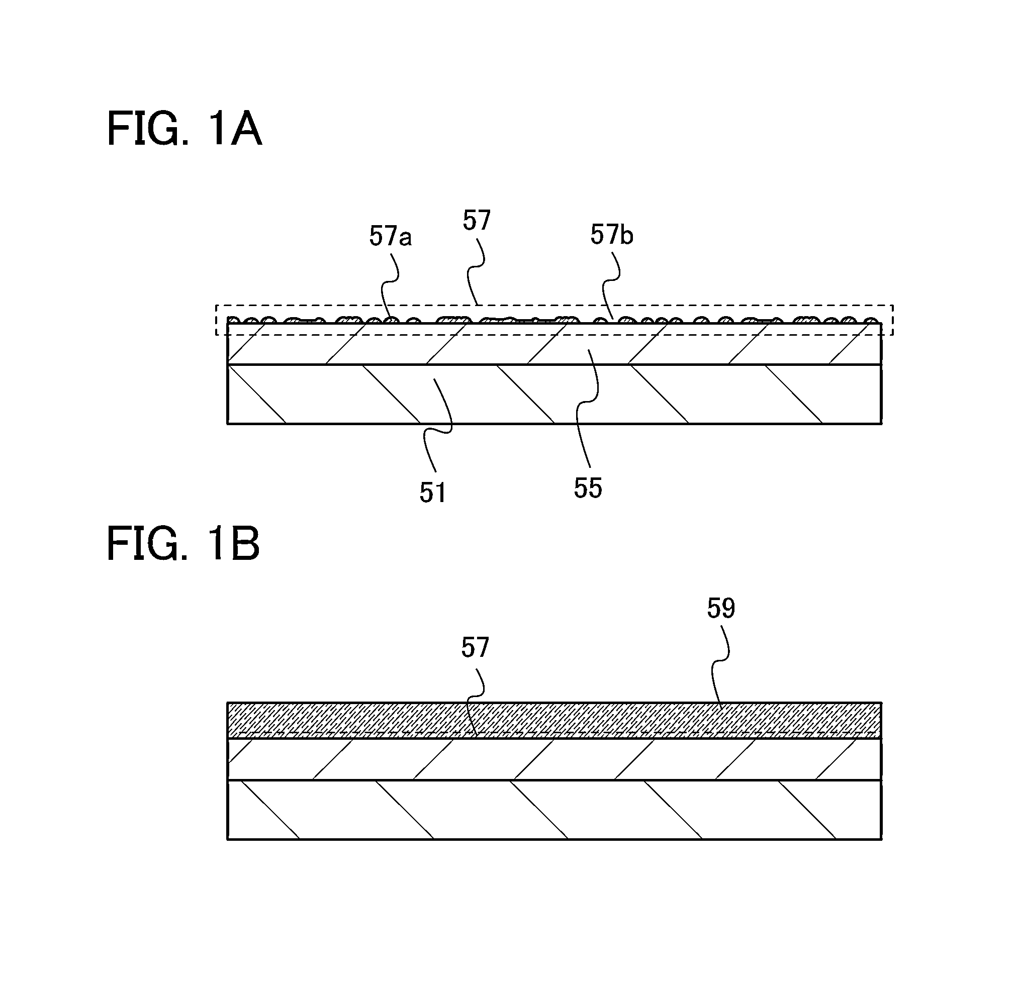
[0044]In this embodiment, a method for forming a microcrystalline semiconductor film in which the crystallinity is improved by reduction of a space between mixed phase grains will be described with reference to FIGS. 1A and 1B and FIG. 2.

[0045]As illustrated in FIG. 1A, an insulating film 55 is formed over a substrate 51, and a seed crystal 57 is formed over the insulating film 55.

[0046]As the substrate 51, a glass substrate, a ceramic substrate, a plastic substrate which has high heat resistance enough to withstand a process temperature of this manufacturing process, or the like can be used. In the case where the substrate does not need a light-transmitting property, a metal substrate, such as a stainless steel substrate, provided with an insulating film on its surface may be used. As the glass substrate, for example, an alkali-free glass substrate of barium borosilicate glass, aluminoborosilicate glass, aluminosilicate glass, or the like may be used. Note that there ...

embodiment 2

(Embodiment 2)

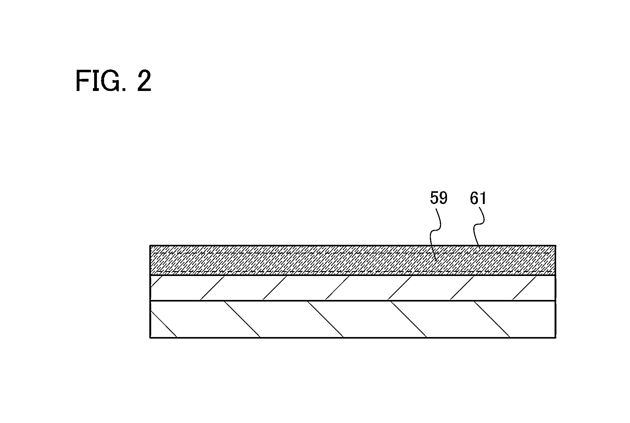
[0076]In this embodiment, a method for forming a microcrystalline semiconductor film having higher crystallinity than the microcrystalline semiconductor film in Embodiment 1 will be described with reference to FIGS. 1A and 1B and FIG. 2.

[0077]As in Embodiment 1, the seed crystal 57 and the microcrystalline semiconductor film 59 are formed through the process of FIGS. 1A and 1B.

[0078]Then, as illustrated in FIG. 2, a second microcrystalline semiconductor film 61 is formed over the microcrystalline semiconductor film 59.

[0079]The second microcrystalline semiconductor film 61 is formed under a third condition in a reaction chamber of the plasma CVD apparatus by glow discharge plasma using a mixture of hydrogen and a deposition gas containing silicon or germanium. Alternatively, the second microcrystalline semiconductor film 61 may be formed under the third condition by glow discharge plasma using a mixture of hydrogen, a deposition gas containing silicon or germanium, and...

embodiment 3

(Embodiment 3)

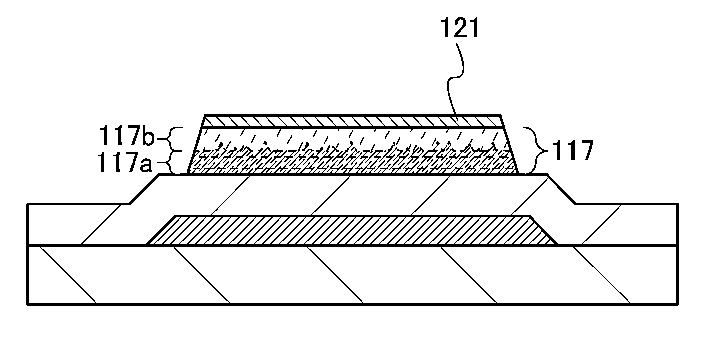
[0082]In this embodiment, a method for manufacturing a thin film transistor formed in a semiconductor device that is one embodiment of the present invention will be described with reference to FIGS. 3A to 3D, FIGS. 4A and 4B, FIGS. 5A to 5C, and FIGS. 6A to 6D. Note that an n-channel thin film transistor has higher carrier mobility than a p-channel thin film transistor. Further, it is preferable that all thin film transistors formed over the same substrate have the same polarity because the number of manufacturing steps can be reduced in such a case. In this embodiment, a method for manufacturing n-channel thin film transistors will be described.

[0083]Note that the term “on-state current” refers to current which flows between a source electrode and a drain electrode when a thin film transistor is on. For example, in the case of an n-channel thin film transistor, the on-state current refers to current which flows between a source electrode and a drain electrode when gat...


PUM

PropertyMeasurementUnit
pressureaaaaaaaaaa
sizeaaaaaaaaaa
sizeaaaaaaaaaa

Abstract

A seed crystal including mixed phase grains having high crystallinity with a low grain density is formed under a first condition, and a microcrystalline semiconductor film is formed over the seed crystal under a second condition which allows the mixed phase grains in the seed crystal to grow to fill a space between the mixed phase grains. In the first condition, the flow rate of hydrogen is 50 times or greater and 1000 times or less that of a deposition gas containing silicon or germanium, and the pressure in a process chamber is greater than 1333 Pa and 13332 Pa or less. In the second condition, the flow rate of hydrogen is 100 times or greater and 2000 times or less that of a deposition gas containing silicon or germanium, and the pressure in the process chamber is 1333 Pa or greater and 13332 Pa or less.

Description

BACKGROUND OF THE INVENTION[0001]1. Field of the Invention[0002]One embodiment of the present invention relates to a method for forming a microcrystalline semiconductor film, a method for manufacturing a semiconductor device including the microcrystalline semiconductor film, and a display device.[0003]In this specification, a semiconductor device means all types of devices which can function by utilizing semiconductor characteristics, and a display device, an electro-optical device, a photoelectric conversion device, a semiconductor circuit, and an electronic device are all semiconductor devices.[0004]2. Description of the Related Art[0005]As one type of field-effect transistor, a thin film transistor whose channel region is formed in a semiconductor film which is formed over a substrate having an insulating surface is known. Techniques in which amorphous silicon, microcrystalline silicon, or polycrystalline silicon is used for the semiconductor film where the channel region is form...

Claims


Application Information

Patent Timeline
Patent Type & Authority Patents(United States)
IPC IPC(8): C30B29/06C30B29/08H01L21/00H01L29/04C30B25/18H01L29/786C30B25/10
CPCH01L29/78618C30B25/105C30B29/06H01L29/78648C30B25/183H01L29/04H01L29/78696C30B29/08
Inventor TAJIMA, RYOTATANAKA, TETSUHIROOHTSUKI, TAKASHITOKUMARU, RYOEGI, YUJIKATO, ERIKAMORIKUBO, MIYAKO
Owner SEMICON ENERGY LAB CO LTD
Why Eureka
Try Eureka