Light emitting device package and method for manufacturing the same

Active Publication Date: 2008-06-26
SUZHOU LEKIN SEMICON CO LTD +1
View PDF10 Cites 53 Cited by
  • Summary
  • Abstract
  • Description
  • Claims
  • Application Information

AI Technical Summary

Benefits of technology

[0024]An object of the present invention is to provide a light emitting device package capable of achieving easy formation of a reflection film adapted to forwardly reflect light laterally emitted from a li

Problems solved by technology

Since GaP is an indirect transition material causing a degradation in efficiency, the green LEDs fabricated using this material cannot practically produce light of pure green.
In this case, the semiconductor is damaged, so that the LED can be no longer used.
In the above-menti

Method used


Image

  • Light emitting device package and method for manufacturing the same
  • Light emitting device package and method for manufacturing the same
  • Light emitting device package and method for manufacturing the same

Examples


first embodiment

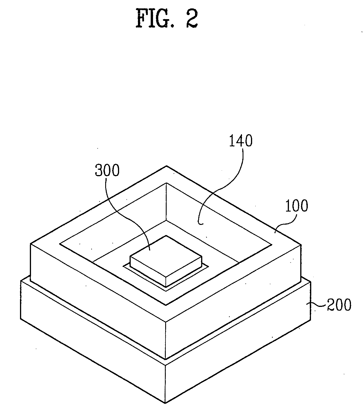
[0056]Referring to FIG. 2, a light emitting device package according to a first embodiment of the present invention is illustrated. The light emitting device package includes an upper substrate 100 and a lower substrate 200. A light emitting device 300 is mounted on the lower substrate 200. The lower substrate 200 is made of a material having a heat transfer coefficient. The upper substrate 100 is bonded to the lower substrate 200, and is provided with a reflection film for forwardly reflecting light emitted from the light emitting device 300.

[0057]The material of the lower substrate 200 may be ceramic such as SiC, AlN, or graphite having a high heat transfer coefficient. Here, the ceramic means a material such as an oxide, nitride, or carbide containing mineral elements as major components. Such a material, namely, the oxide, nitride or carbide, may be used for the lower substrate 200.

[0058]In addition, PCB, BeO, SiO, Si, Al, AlOx, PSG, a synthetic resin (plastic) material such as ...

second embodiment

[0098]Referring to FIGS. 13 and 14, a light emitting device package according to a second embodiment of the present invention is illustrated. The light emitting device package includes an upper substrate 500 and a lower substrate 600. A light emitting device 300 is mounted on the lower substrate 600. The upper substrate 500 is bonded to the lower substrate 600, and is provided with a reflection film 510 for forwardly reflecting light emitted from the light emitting device 300.

[0099]In the lower substrate 600, which may be a silicon substrate, zener diodes 610 are formed to achieve an improvement in the voltage withstand characteristics of the light emitting device 300.

[0100]A molding epoxy resin may be used for the upper substrate 500.

[0101]The upper substrate 500 or lower substrate 600 may be made of a material selected from PCB, BeO, SiO, Si, Al, AlOx, PSG, a synthetic resin (plastic) material such as epoxy resin, ceramic, and Al2O3.

[0102]Through holes 620 may be formed through th...

third embodiment

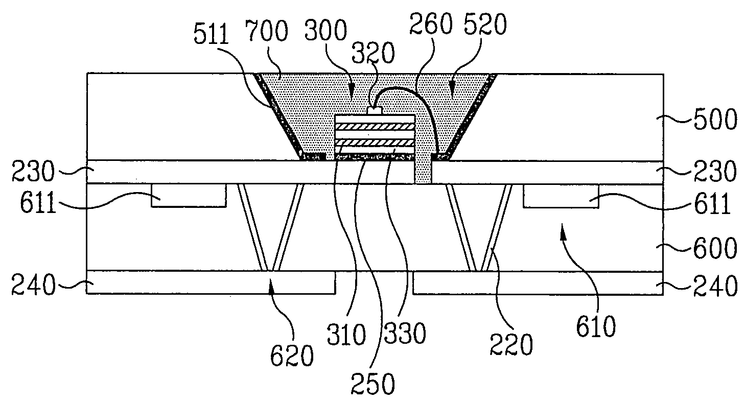
[0114]Referring to FIG. 16, a light emitting device package according to a third embodiment of the present invention is illustrated. The light emitting device package includes an upper substrate 500 and a lower substrate 600. The lower substrate 600 is made of semiconductor such as silicon, and is formed with through holes 620 each having an inclination in one direction. The upper substrate 500 is formed with a mounting hole 520 for mounting a light emitting device 300.

[0115]The upper substrate 500 or lower substrate 600 may be made of a material selected from PCB, BeO, SiO, Si, Al, AlOx, PSG, a synthetic resin (plastic) material such as epoxy resin, ceramic, and Al2O3.

[0116]A reflection film 511 is formed around the light emitting device 300. The reflection film 511 may extend along the inner side wall surface of the mounting hole 520 and the surface of the mounting hole 520 where the light emitting device 300 is mounted.

[0117]Each through hole 620 of the lower substrate 600 can be...


PUM


Abstract

A light emitting device package capable of achieving an enhancement in light emission efficiency and a reduction in thermal resistance, and a method for manufacturing the same are disclosed. The method includes forming a mounting hole in a first substrate, forming through holes in a second substrate, forming a metal film in the through holes, forming at least one pair of metal layers on upper and lower surfaces of the second substrate such that the metal layers are electrically connected to the metal film, bonding the first substrate to the second substrate, and mounting at least one light emitting device in the mounting hole such that the light emitting device is electrically connected to the metal layers formed on the upper surface of the second substrate.

Description

[0001]This application claims the benefit of Korean Patent Application No. 10-2006-0131732, filed on Dec. 21, 2006, which is hereby incorporated by reference as if fully set forth herein.BACKGROUND OF THE INVENTION[0002]1. Field of the Invention[0003]The present invention relates to a light emitting device package and a method for manufacturing the same, and more particularly, to a light emitting device package capable of achieving an enhancement in light emission efficiency and a reduction in thermal resistance, and a method for manufacturing the same.[0004]2. Discussion of the Related Art[0005]Light emitting diodes (LEDs) are well known as a semiconductor light emitting device which converts current to light, to emit light. Since a red LED using GaAsP compound semiconductor was commercially available in 1962, it has been used, together with a GaP:N-based green LED, as a light source in electronic apparatuses, for image display.[0006]The wavelength of light emitted from such an LED...

Claims


Application Information

Patent Timeline
IPC IPC(8): H01L33/00H01L33/50H01L33/32H01L33/60H01L33/62H01L33/64
CPCH01L25/0753H01L25/167H01L2924/10253H01L2224/73265H01L2224/48091H01L23/62H01L2224/45139H01L33/486H01L33/62H01L2924/00014H01L2924/00H01L2224/45015H01L2924/207
Inventor KIM, GEUN HOLEE, SEUNG YEOBWON, YU HO
Owner SUZHOU LEKIN SEMICON CO LTD
Why Eureka
Try Eureka