Ferroelectric memory array for implementing a zero cancellation scheme to reduce plateline voltage in ferroelectric memory

Active Publication Date: 2008-06-26
TEXAS INSTR INC
View PDF23 Cites 14 Cited by
  • Summary
  • Abstract
  • Description
  • Claims
  • Application Information

AI Technical Summary

Benefits of technology

[0018]The memory array cells and zero cancellation circuits may be constructed as a multilayer structure with conductive contacts formed between layers, wherein at least one layer of the zero cancellation circuit is identical or substantially identical (e.g., similar) to that of the individual ferroelectric memory cells. In one example, the multi-layer structure comprises four layers, with the cell transistors, the zero cancellation switching devices, and the zero cancellation discharge switching devices being formed on or in a semiconductor body in a first layer, and with array wordlines extending along rows of ferroelectric memory cells, a zero cancellation wordline extending along the zero cancellation circuits, and a zero cancellation discharge wordline extending along the zero cancellation circuits in the first layer. A second layer comprises the ferroelectric cell capacitors and the zero cancellation capacitors, a third layer comprises array platelines ext

Problems solved by technology

Since reading the cell data is a destructive operation, the sensed data is then restored to the target memory cell following each read operation.
For low power devices, however, the supply level Vdd may not be this high.
Since the saturation voltage of a ferroelectric capacitor is dependent upon the ferroelectric materia

Method used


Image

  • Ferroelectric memory array for implementing a zero cancellation scheme to reduce plateline voltage in ferroelectric memory
  • Ferroelectric memory array for implementing a zero cancellation scheme to reduce plateline voltage in ferroelectric memory
  • Ferroelectric memory array for implementing a zero cancellation scheme to reduce plateline voltage in ferroelectric memory

Examples


first embodiment

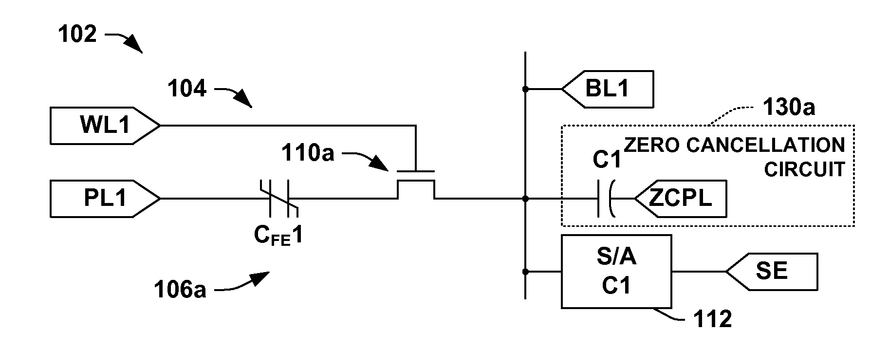
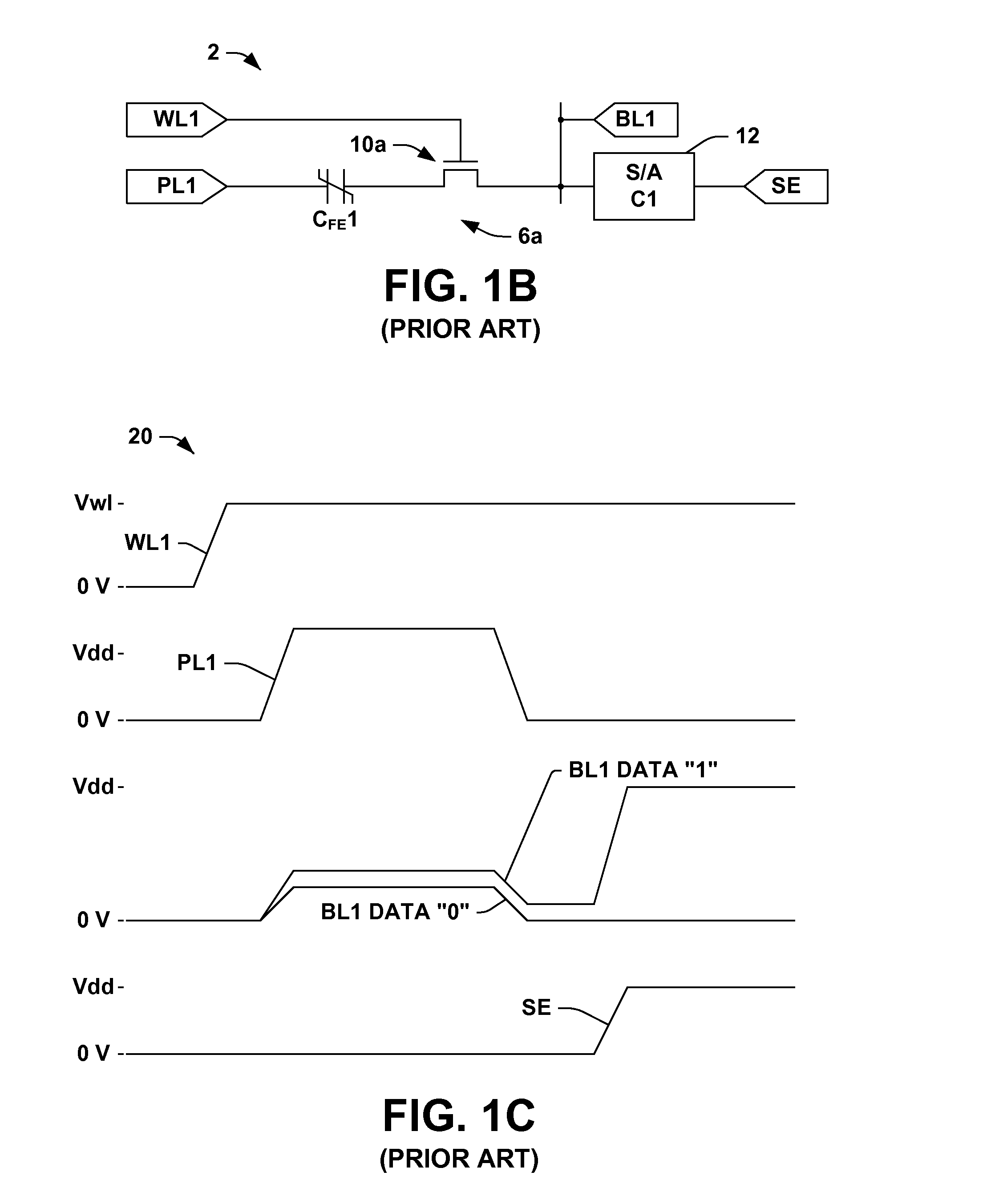
[0070]In the invention, FIGS. 5A-5E illustrate a portion of the exemplary ferroelectric memory device 102 of FIGS. 2A-3G above. FIGS. 5A and 5B are partial sectional side elevation views and FIGS. 5C-5E are partial sectional top plan views, wherein the views of FIGS. 5A and 5B are taken along lines 5A-5A and 5B-5B, respectively, in FIGS. 5C-5E and the views of FIGS. 5C, 5D, and 5E are taken along lines 5C-5C, 5D-5D, and 5E-5E, respectively, in FIGS. 5A and 5B. In particular, FIG. 5A illustrates a portion of a capacitor under bitline layout of several exemplary ferroelectric memory cells 106 of the array 104 in the device 102 (shown in the top portions of FIGS. 5C-5E) and FIG. 5B illustrates a portion of an exemplary zero cancellation system 130 in one or more rows formed near the memory array 104 (bottom portions of FIGS. 5C-5E).

[0071]As illustrated in FIGS. 5A and 5B, the device 102 is constructed as a multi-layer structure with a first layer shown in FIG. 5C, second and third laye...

second embodiment

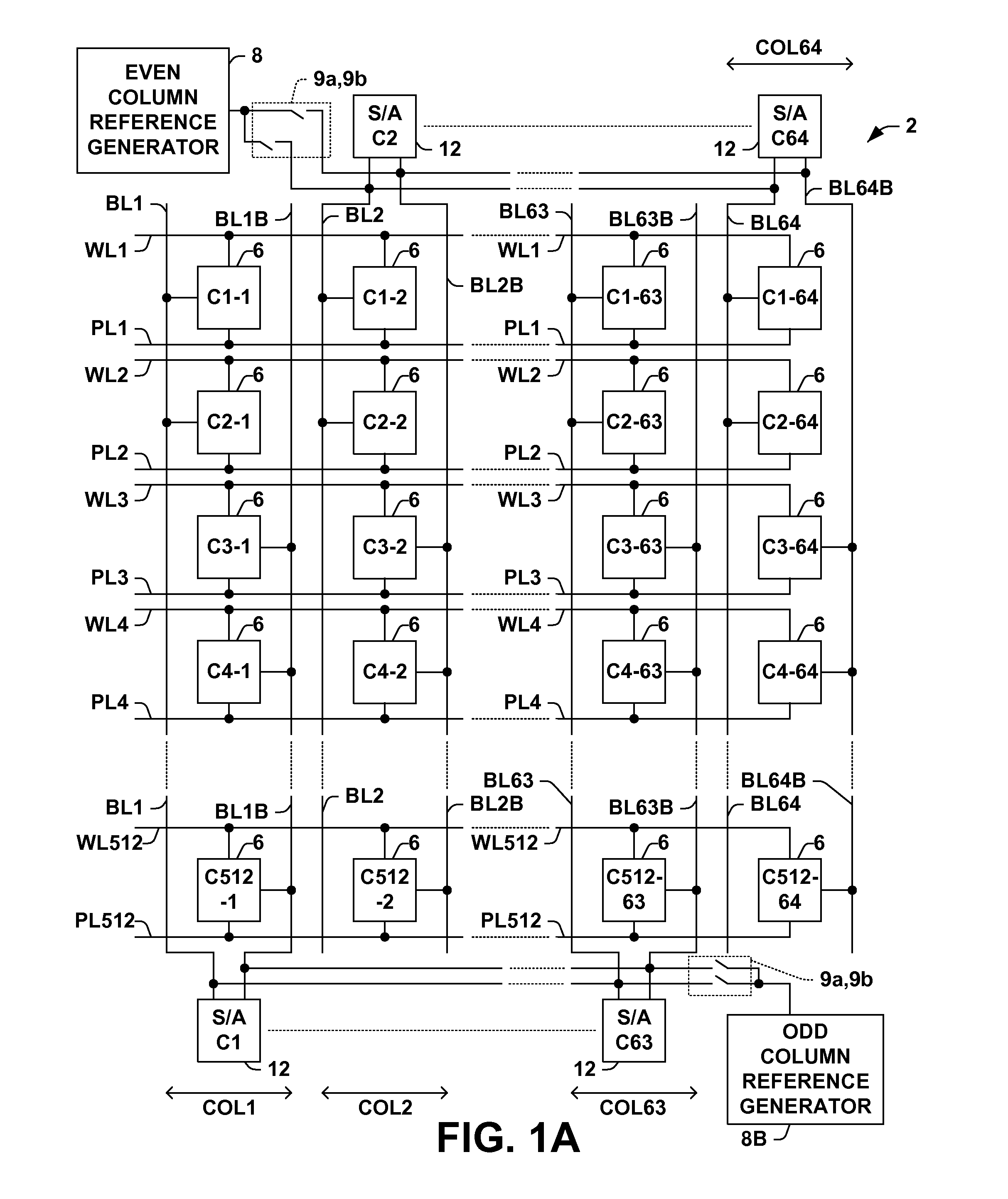
[0080]In the second embodiment, moreover, the zero cancellation circuit 130a further comprises the zero cancellation discharge switching device 136 (schematically illustrated in FIG. 3B) formed in the second super cell 309b (shown in the right half of FIG. 6A). The super cell 309b is substantially identical to the memory super cells 309, with a few minor alterations. One difference is that the bitline connection of the modified super cell 309b is omitted in the third layer, indicated as a dashed circle location “A” in FIGS. 6A and 6E, and the corresponding third layer landing pad structure of the memory super cell is replaced by a first metal level (M1) routing 330 for the pre-determined voltage level (Vss) to which the zero cancellation capacitor C1 is coupled by the switching device 136 (labeled VSS in FIG. 6D). Other equivalent modifications could be done to couple the shared source / drain in the super cell 309b to Vss or other pre-determined voltage level instead of to the associ...


PUM


Abstract

Memory devices are provided, having a ferroelectric memory array and a zero cancellation system with one or more zero cancellation circuits for coupling a negative charge to a memory array bitline through a zero cancellation capacitor while a memory cell plateline signal is applied during a read operation, wherein one or more layers of the zero cancellation system layout is identical or substantially identical to that of the memory cells of the array.

Description

REFERENCE TO RELATED APPLICATIONS[0001]This application claims priority to Ser. No. 60 / 877,203 filed Dec. 26, 2006, which is entitled “Ferroelectric Memory Array for Implementing a Zero Cancellation Scheme to Reduce Plateline Voltage in Ferroelectric Memory.”FIELD OF INVENTION[0002]The present invention relates generally to semiconductor devices and more particularly to improved apparatus and methods for reduced plateline voltages in ferroelectric memory devices.BACKGROUND OF THE INVENTION[0003]In semiconductor memory devices, data is read from or written to memory cells in the device according to decoded address information and various other control signals. Such memory devices are used for storage of data and / or program code in personal computer systems, embedded processor-based systems, video image processing circuits, communications devices, and the like. Ferroelectric memory devices are integrated circuits (ICs), such as dedicated memories or other ICs in which data is stored i...

Claims


Application Information

Patent Timeline
IPC IPC(8): G11C11/22
CPCG11C11/22
Inventor MADAN, SUDHIR KUMAR
Owner TEXAS INSTR INC
Why Eureka
Try Eureka