Semiconductor device and method for fabricating the same

Inactive Publication Date: 2008-07-03
SK HYNIX INC
View PDF3 Cites 12 Cited by
  • Summary
  • Abstract
  • Description
  • Claims
  • Application Information

AI Technical Summary

Benefits of technology

[0009]Embodiments of the present invention are directed to providing a capacitor suitable for fabrication and having good electri

Problems solved by technology

When the lower electrode is formed of polysilicon, it is difficult to use Ta2O5 for forming the dielectric layer since the lower electrode formed of polysilicon oxidizes when a high-temperature heat treatment is performed on the dielectric layer formed of Ta2O5.
Furthermore, the electric characteristics of the capacitor deteriorate due to variations in the current output of the capacitor caused by asymmetric current-voltage characteristics of the capacitor.
However, a ruthenium layer deposited on a substrate by ALD is not fi

Method used


Image

  • Semiconductor device and method for fabricating the same
  • Semiconductor device and method for fabricating the same
  • Semiconductor device and method for fabricating the same

Examples


first embodiment

[0025]A method for depositing a ruthenium layer by atomic layer deposition (ALD) and a method for depositing a ruthenium oxide layer by ALD will now be described with reference to FIGS. 3 and 4, and a method for fabricating a capacitor will be described in accordance with the present invention.

[0026]FIG. 3 illustrates a method for depositing a ruthenium layer by ALD and FIG. 4 illustrates a method for depositing a ruthenium oxide layer by ALD.

[0027]Referring to FIG. 3, the method for depositing a ruthenium layer by ALD may include a first process for injecting a ruthenium source into a reaction chamber, a second process for purging the reaction chamber using N2 gas, a third process for injecting reaction gas containing O2 or O3 into the reaction chamber, and a fourth process for purging the reaction chamber using N2 gas to remove inactive gas that does not participate in a reaction.

[0028]A cycle of the first to fourth processes can be repeated to deposit a uniform thin layer to a gi...

second embodiment

[0055]Based on the reduction of a ruthenium oxide layer explained with reference to FIG. 6, a method for fabricating a capacitor will now be described in accordance with the present invention.

[0056]FIGS. 7A to 7F illustrate a method for fabricating a capacitor in accordance with a second embodiment of the present invention. In FIGS. 5A to 5G and 7A to 7F, like reference numerals denote like elements. Thus, in the following description, like elements will not be described in detail.

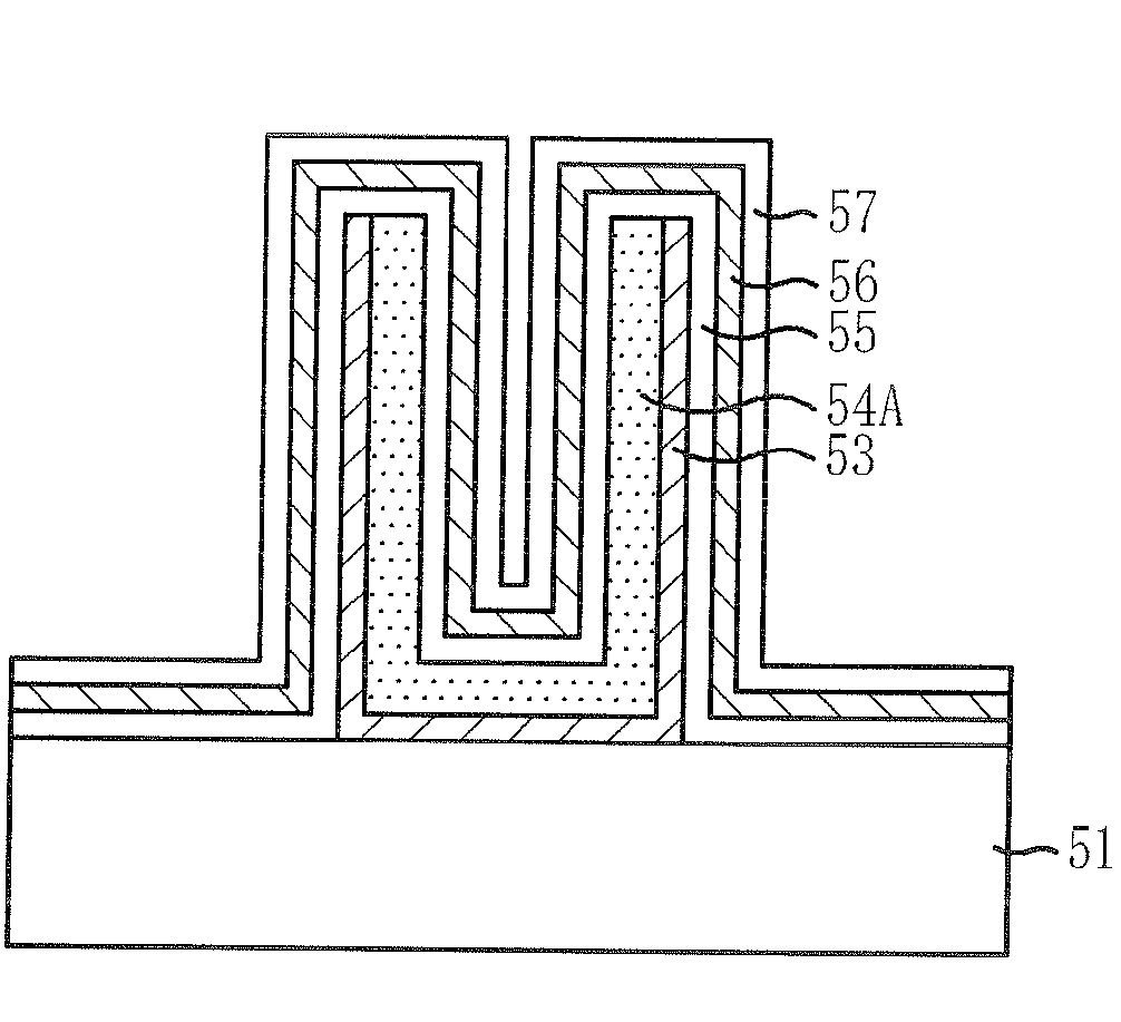
[0057]Referring to FIG. 7A, a mold oxide layer 52 defining a capacitor region is formed on a substrate 51 including a lower structure, and a first ruthenium oxide layer 53 is deposited on the entire surface of the substrate 51 including the mold oxide layer 52.

[0058]The first ruthenium oxide layer 53 may be deposited in the same method as described with reference to FIG. 5C except that the first ruthenium oxide layer 53 is deposited to a relatively small thickness so as to allow the first ruthenium oxide l...


PUM


Abstract

A capacitor includes a lower electrode, a dielectric layer, an upper electrode, and a ruthenium oxide layer. At least one of the lower electrode and the upper electrode is formed of a ruthenium layer, and the ruthenium oxide layer is disposed next to the ruthenium layer.

Description

CROSS-REFERENCE TO RELATED APPLICATIONS[0001]The present invention claims priority of Korean patent application numbers 10-2006-0134290 and 10-2007-0098562, filed on Dec. 27, 2006, and Oct. 1, 2007, respectively, which are incorporated by reference in their entirety.BACKGROUND OF THE INVENTION[0002]The present invention relates to a method for fabricating a capacitor of a semiconductor device, and more particularly, to a capacitor including a metal layer such as a ruthenium (Ru) layer that is used for a lower or an upper electrode, and a method for fabricating the capacitor.[0003]In general, a capacitor used in a memory cell may include a lower electrode for storage, a dielectric layer, and an upper electrode for a plate. The capacitance of the capacitor can be increased by, for example, reducing a thickness of the dielectric layer, forming the capacitor into a three-dimensional shape to increase the effective area of the capacitor, or using a high-permittivity dielectric material s...

Claims


Application Information

Patent Timeline
IPC IPC(8): H01L29/92H01L21/02
CPCH01L28/65
Inventor DO, KWAN-WOOROH, JAE-SUNGLEE, KEE-JEUNGKIL, DEOK-SINKIM, YOUNG-DAEKIM, JIN-HYOCKPARK, KYUNG-WOONGSONG, HAN-SANG
Owner SK HYNIX INC
Why Eureka
Try Eureka