Metalorganic chemical vapor deposittion (MOCVD) growth of high performance non-polar III-nitride optical devices

Active Publication Date: 2008-07-10
JAPAN SCI & TECH CORP
View PDF24 Cites 63 Cited by
  • Summary
  • Abstract
  • Description
  • Claims
  • Application Information

AI Technical Summary

Benefits of technology

[0047]The device is grown on a low defect density substrate. This substrate can be a bulk m-plane GaN substrate grown by hydride vapor phase epitaxy (HVPE) or an m-plane sidewall lateral epitaxial overgrowth (SLEO)

Problems solved by technology

The slanted quantum wells consequently diminish the spatial overlap of the hole and electron wavefunctions, in turn decreasing radiative recombination efficiency.
The main reason for this p

Method used


Image

  • Metalorganic chemical vapor deposittion (MOCVD) growth of high performance non-polar III-nitride optical devices
  • Metalorganic chemical vapor deposittion (MOCVD) growth of high performance non-polar III-nitride optical devices
  • Metalorganic chemical vapor deposittion (MOCVD) growth of high performance non-polar III-nitride optical devices

Examples


Embodiment Construction

[0058]In the following description of the preferred embodiment, reference is made to the accompanying drawings which form a part hereof, and in which is shown by way of illustration a specific embodiment in which the invention may be practiced. It is to be understood that other embodiments may be utilized and structural changes may be made without departing from the scope of the present invention.

[0059]Overview

[0060]The present invention describes how to grow state of the art m-plane GaN optical devices. The techniques depicted herein have been used to achieve improved m-plane GaN LED performance. These m-plane GaN LEDs have comparable output powers to the best quality c-plane GaN LEDs currently in existence. Such results represent a major breakthrough in optoelectronic devices.

[0061]Technical Description

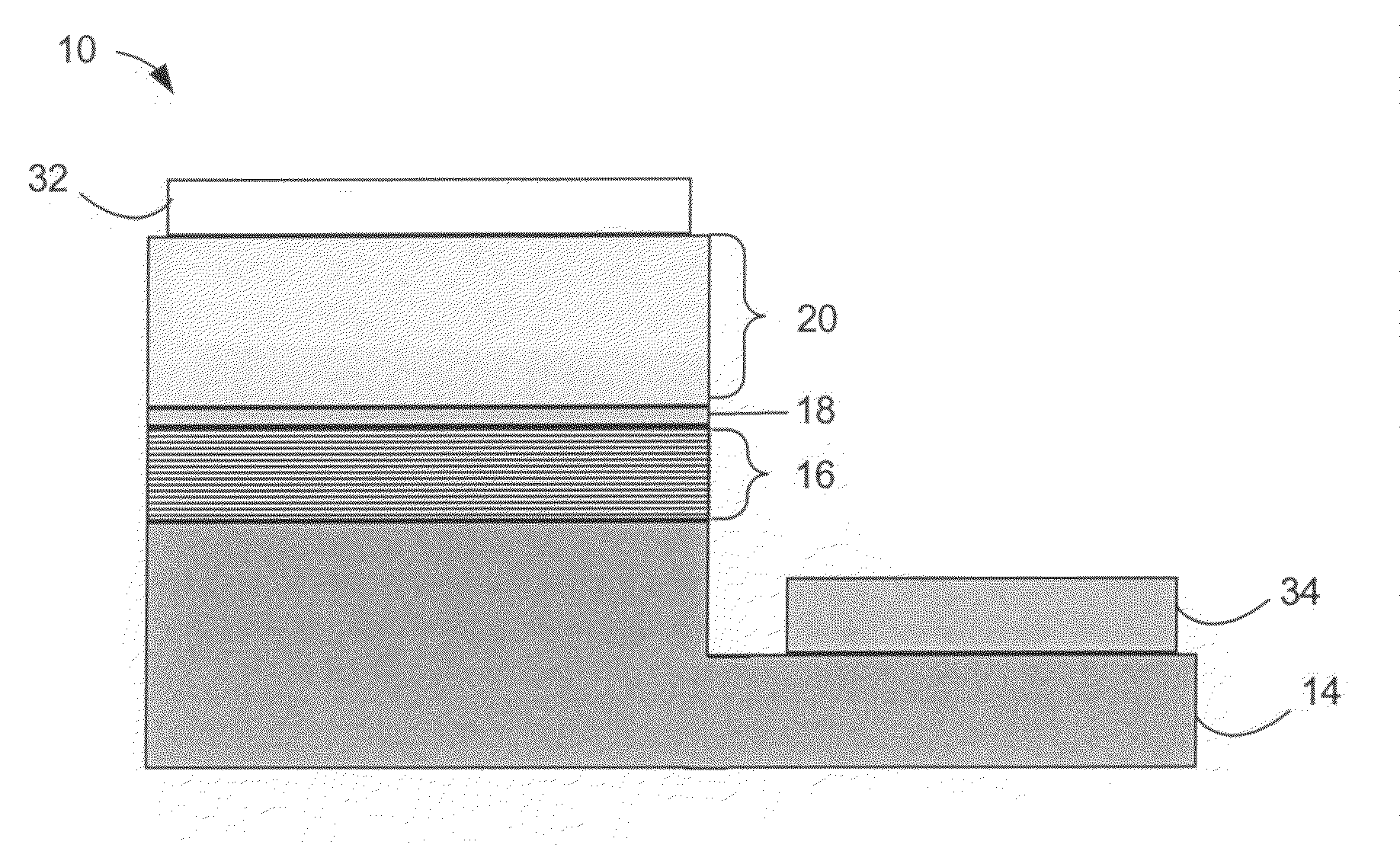
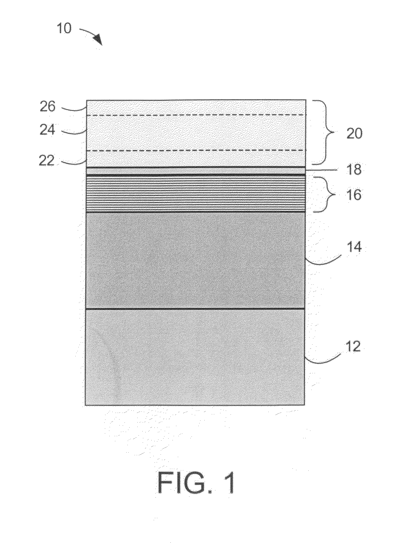
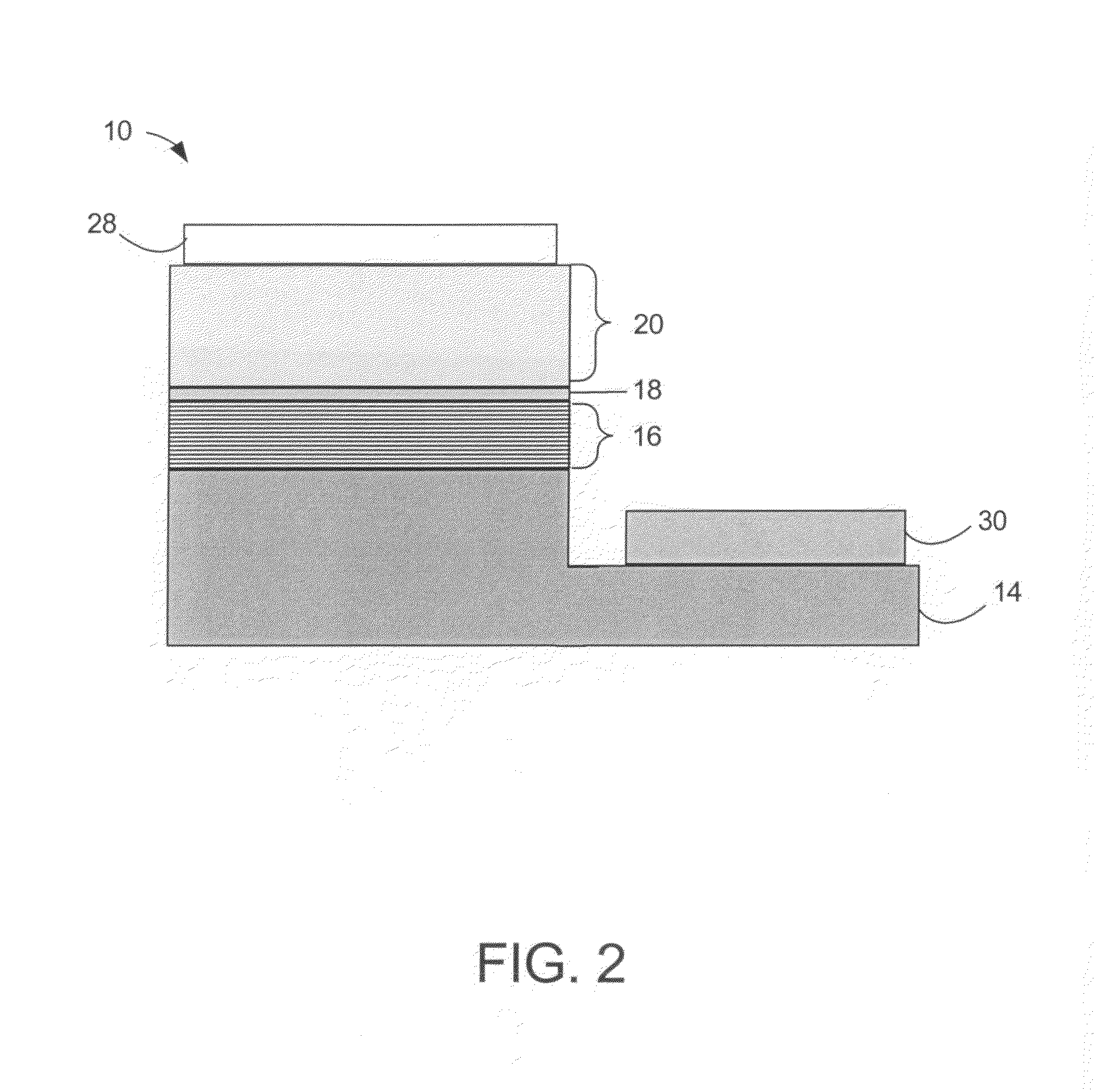
[0062]The high performance m-plane GaN LEDs of the present invention are grown on ultra-low defect density substrates or templates. These substrates or templates can be, but are not...


PUM


Abstract

A method of device growth and p-contact processing that produces improved performance for non-polar III-nitride light emitting diodes and laser diodes. Key components using a low defect density substrate or template, thick quantum wells, a low temperature p-type III-nitride growth technique, and a transparent conducting oxide for the electrodes.

Description

CROSS-REFERENCE TO RELATED APPLICATIONS[0001]This application claims the benefit under 35 U.S.C. Section 119(e) of the following co-pending and commonly-assigned U.S. patent application:[0002]U.S. Provisional Application Ser. No. 60 / 869,535, filed on Dec. 11, 2006, by Mathew C. Schmidt, Kwang Choong Kim, Hitoshi Sato, Steven P. DenBaars, James S. Speck, and Shuji Nakamura, entitled “MOCVD GROWTH OF HIGH PERFORMANCE M-PLANE GAN OPTICAL DEVICES,” attorneys' docket number 30794.212-US-P1 (2007-316-1);[0003]which application is incorporated by reference herein.[0004]This application is related to the following co-pending and commonly-assigned applications:[0005]U.S. Utility application Ser. No. 10 / 581,940, filed on Jun. 7, 2006, by Tetsuo Fujii, Yan Gao, Evelyn. L. Hu, and Shuji Nakamura, entitled “HIGHLY EFFICIENT GALLIUM NITRIDE BASED LIGHT EMITTING DIODES VIA SURFACE ROUGHENING,” attorney's docket number 30794.108-US-WO (2004-063), which application claims the benefit under 35 U.S.C ...

Claims


Application Information

Patent Timeline
IPC IPC(8): H01L33/00H01L21/00
CPCB82Y20/00H01L21/0237H01L21/02389H01L21/02458H01S2304/04H01L21/0254H01L33/0075H01S5/34333H01L21/02507
Inventor SCHMIDT, MATHEW C.KIM, KWANG CHOONGSATO, HITOSHIDENBAARS, STEVEN P.SPECK, JAMES S.NAKAMURA, SHUJI
Owner JAPAN SCI & TECH CORP
Why Eureka
Try Eureka