Very low profile multilayer components

a multi-layer, low-profile technology, applied in the direction of fixed capacitors, stacked capacitors, fixed capacitor details, etc., can solve the problems of difficult control of termination application, significant high cost factor of multi-layer devices, so as to reduce inductance and resistance, the effect of facilitating testing

Inactive Publication Date: 2008-07-10
AVX CORP
View PDF23 Cites 31 Cited by
  • Summary
  • Abstract
  • Description
  • Claims
  • Application Information

AI Technical Summary

Benefits of technology

[0029]In another present exemplary embodiment, a low inductance controlled equivalent series resistance (ESR) multilayer capacitor is provided having at least first and second pairs of electrodes, and having a plurality of dummy tabs. Preferably, such at least first pair of electrodes may comprise interdigitated electrodes having a respective end tab on opposite ends thereof, to reduce inductance and resistance, and to provide for ease of testing during the manufacturing process. Still further, such first pair of electrodes may preferably have respective side tabs interdigitated with those of the other interdigitated electrode. Such at least second pair of electrodes preferably has a respective end tab on opposite ends thereof. Such dummy tabs preferably are formed adjacent such electrodes but not electrically connected thereto, to provide support and nucleation points for electroless copper termination.

Problems solved by technology

The use of multiple sets of silk screen masks to produce differing alternate layers for multilayered devices represents a significant cost factor in the production of multilayered devices.
Further, terminations commonly used with such multilayer devices consume a significant portion of the vertical height of the finished products.
The application of terminations is often hard to control and can become problematic with reduction in chip sizes or with close features.
The ever-shrinking size of electronic components makes it quite difficult to print termination stripes in a predetermined area with required precision.
Ever smaller spacing brought on by reduced component size or an increased number of termination contacts for an electronic chip device may cause the resolution limits of typical termination machines to become a limiting factor to further reductions.
Other problems that can arise when trying to apply patterned terminations with thick film processes include shifting of the termination lands, incorrect positioning of terminations such that internal electrode tabs are exposed or missed entirely, and missing wrap-around termination portions.
Yet further problems may be caused when too thin a coating of the paint-like termination material is applied or when one portion of termination coating smears into another causing shorted termination lands.
Another problem of the thick film systems is that it is often difficult to form termination portions on only selected sides of a device, such as on a vertical surface.
While various aspects and alternative features are known in the field of multilayer electronic components and terminations thereof, no one design has emerged that generally addresses all of the issues as discussed herein.

Method used


Image

  • Very low profile multilayer components
  • Very low profile multilayer components
  • Very low profile multilayer components

Examples


first embodiment

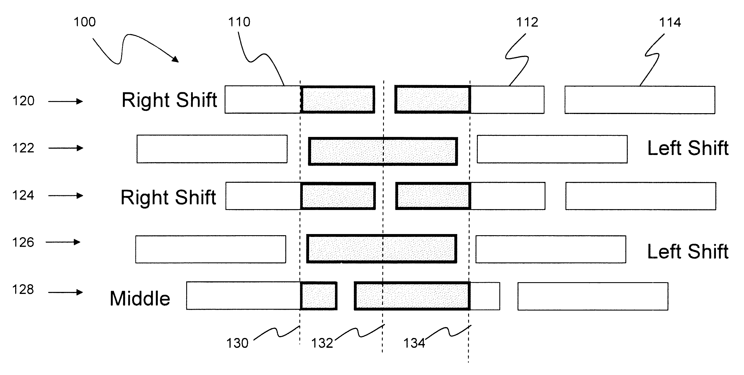
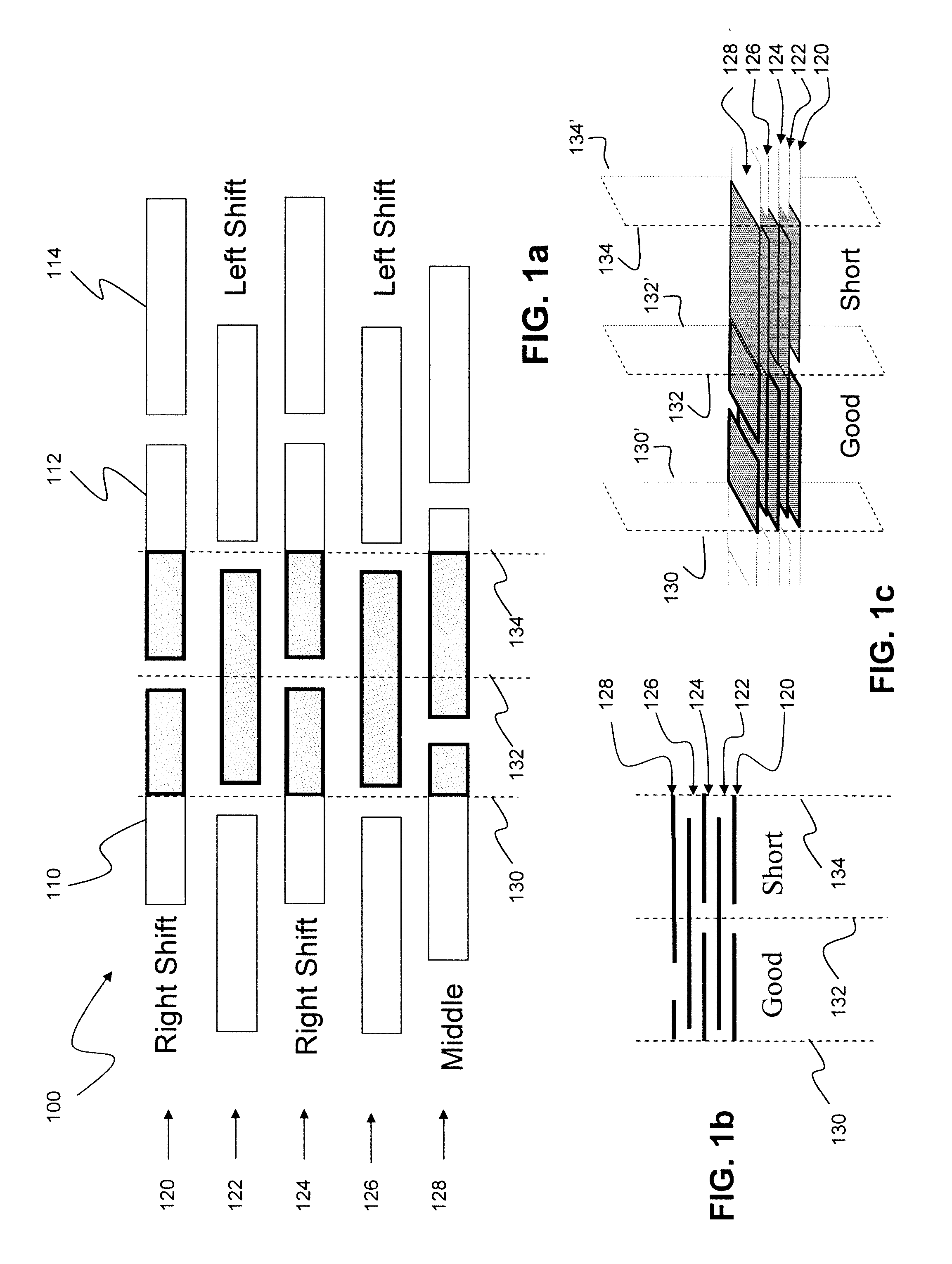
[0085]With reference to FIG. 4a, it will be seen that a first electrode layer 120′ is printed on un-illustrated dielectric material with the screen printing mask 100 positioned in a central or middle location. The second electrode layer 122′ is printed after the screen printing mask 100 has been shifted to the left relative to the middle position of layer 120′. The next electrode layer 124′ is printed following return of the screen printing mask 100 to the same central or middle position it had occupied for the printing of layer 120′. Electrode layer 126′ is produced with a left shift of the screen printing mask 100 to the same position occupied by the mask for printing of electrode layer 122′. Finally screen printing mask 100 is repositioned to the same central or middle position it previously occupied for the printing of electrode layers 120′ and 124′ so that electrode layer 128′ may be printed. As with the present subject matter, it should be kept in mind that the actually provid...

third exemplary embodiment

[0090]With reference now to FIGS. 5a-5h, the present subject matter will now be described. This third exemplary embodiment of the present subject matter again employs a single screen printing mask 500 defined by a plurality of identical printing openings 510, 512, and 514, portions of some of which are again illustrated in shading to more clearly delineate those portions that will correspond to electrode layers. In a manner similar to the previously described second exemplary embodiment, the third exemplary embodiment employs masks 500 that are positioned in only one of two specific locations to produce the desired devices. In this instance, the devices produced have different electrical and physical characteristics than the devices described with respect to the first and second exemplary embodiments in that feedthrough and Pi filter structures may be created, as will be explained further with respect to FIGS. 5f and 5h.

[0091]As illustrated in FIG. 5a, in a first lateral position r...

fourth exemplary embodiment

[0099]With reference now to FIGS. 6a-6h, the present subject matter will now be described. This fourth exemplary embodiment of the present subject matter again employs a single screen printing mask 600 defined by a plurality of identical printing openings 610, 612, portions of some of which are again illustrated in shading to more clearly delineate those portions that will correspond to electrode layers. In a manner similar to the previously described second exemplary embodiment, the fourth exemplary embodiment employs masks 600 that are positioned in only one of two specific locations to produce the desired devices. The two mask positions in this embodiment are, however, somewhat different from previously discussed embodiments in that the two mask positions are reached by translation of the mask in both a lateral and vertical direction.

[0100]In this instance, the devices produced have different electrical and physical characteristics than the devices described with respect to the f...


PUM

PropertyMeasurementUnit
thickaaaaaaaaaa
thicknessaaaaaaaaaa
thickaaaaaaaaaa

Abstract

Methodologies are disclosed for producing multilayer electronic devices using a single screen printing mask. Plural layer devices are constructed by placing a common mask in alternating positions among alternating layers of support material such that, upon stacking of the plural layers, complimentary electrode structure is produced in alternating layers. Support material may be varied to produce different devices, including capacitors, resistors, and varistors. Multilayer electronic devices include multiple layers providing adjacent printed complimentary electrode layers having an upper surface, a lower surface, a front edge, and a back edge, and with lateral end portions of combined first and second layers trimmed so as to expose selected conductive patterns. Termination material is applied to at least such trimmed lateral end portions. A low inductance controlled equivalent series resistance (ESR) multilayer capacitor, includes at least two different pairs of electrodes, some of which have interdigitated respective side tabs. Termination material may be associated with such electrodes. In some instances, some electrodes may have dummy or anchor tabs associated with them but not electrically connected with them, to facilitate the formation of termination material at designated locations.

Description

PRIORITY CLAIM[0001]This application claims priority under 35 U.S.C.119(e) of Provisional Patent Application Ser. No. 60 / 878,963 filed Jan. 5, 2007, entitled “Very Low Profile Multi-Layer Capacitor;” Provisional Patent Application Ser. No. 60 / 937,474 filed Jun. 28, 2007, entitled “Very Low Profile Multi-Layer Capacitor;” and Provisional Patent Application Ser. No. 60 / 994,353 filed Sep. 19, 2007, entitled “Low Inductance Thin Capacitors” all of which are hereby incorporated by reference in their entirety.FIELD OF THE INVENTION[0002]The present subject matter generally concerns improved component formation for multilayer electronic components. More particularly, the present subject matter relates to methodologies for providing very thin capacitor structures suitable for use with smart card technology. The subject technology utilizes selective placement of a single electrode mask and specialized termination methodologies to fabricate very thin components.BACKGROUND OF THE INVENTION[000...

Claims


Application Information

Patent Timeline
Patent Type & Authority Applications(United States)
IPC IPC(8): H01G4/005H05K1/16
CPCH01C7/1006H01C7/18Y10T29/49155H01G4/005H01G4/30H01C17/065H01G4/012
Inventor BEROLINI, MARIANNEGALVAGNI, JOHN L.RITTER, ANDREW P.
Owner AVX CORP
Why Eureka
Try Eureka