Carrier For Double-Side Polishing Apparatus, Double-Side Polishing Apparatus And Double-Side Polishing Method Using The Same

a polishing apparatus and a carrier technology, applied in the direction of cutting machines, manufacturing tools, edge grinding machines, etc., can solve the problems of short life of the carrier, high cost, inferior product quality, etc., and achieve the effect of high carrier strength, contamination of a wafer such as a silicon wafer, and contamination of the carrier itsel

Inactive Publication Date: 2008-07-10
SHIN-ETSU HANDOTAI CO LTD
View PDF17 Cites 38 Cited by
  • Summary
  • Abstract
  • Description
  • Claims
  • Application Information

AI Technical Summary

Benefits of technology

[0008]The present invention was conceived in view of the above problems. The object of the present invention is to provide a carrier in which the strength of the carrier itself is ...

Problems solved by technology

However, as for a carrier made of glass-epoxy material, abrasion degree during polishing is high, so that the life of the carrier is short and costs run up.
Moreover, the carrier made of glass-epoxy material requires much time to start up, so that the productivity is inferior.
And, as for a carrier made of uncoated SUS material, there is the danger that the semiconductor wafer is con...

Method used


Image

  • Carrier For Double-Side Polishing Apparatus, Double-Side Polishing Apparatus And Double-Side Polishing Method Using The Same
  • Carrier For Double-Side Polishing Apparatus, Double-Side Polishing Apparatus And Double-Side Polishing Method Using The Same
  • Carrier For Double-Side Polishing Apparatus, Double-Side Polishing Apparatus And Double-Side Polishing Method Using The Same

Examples


examples 3 and 4

, COMPARATIVE EXAMPLES 2 AND 3

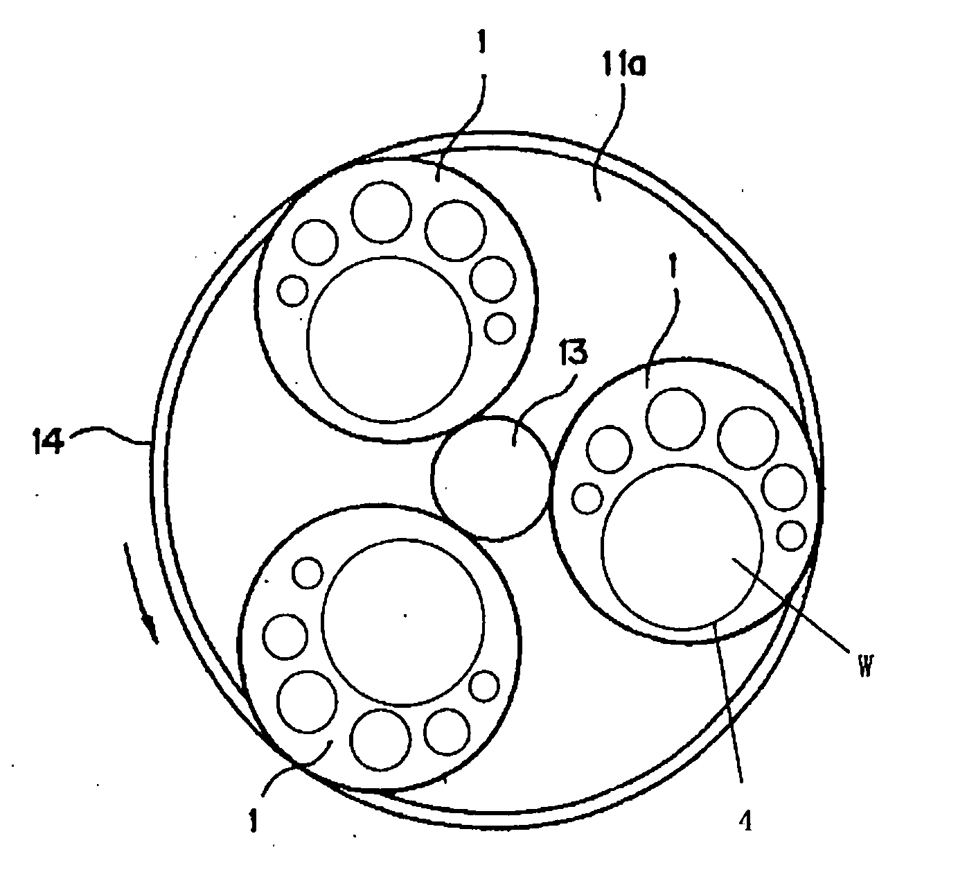
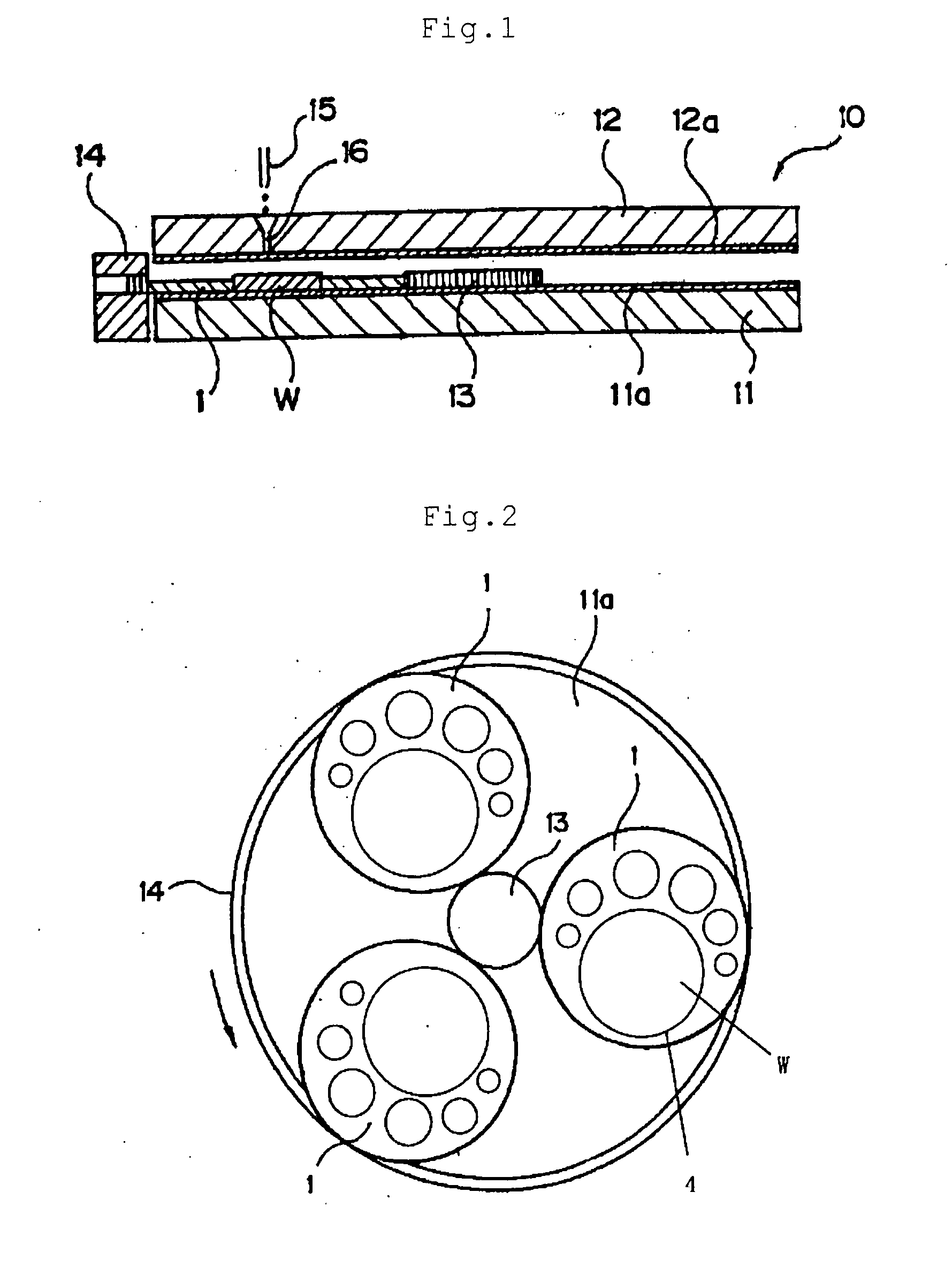
[0066]Next, a silicon wafer with a diameter of 300 mm was prepared as a sample wafer. Then, this silicon wafer was held with a carrier, and both sides of the silicon wafer were polished for 60 minutes using such a double-side polishing apparatus as shown in FIGS. 1 and 2.

[0067]Subsequently, the polished sample wafer was put in a bag, then a mixed solution of nitric acid and hydrofluoric acid was added in the bag and boiled, then impurities in a liquid in the bag were analyzed with ICP-MS.

[0068]A carrier made of uncoated titanium (Examples 3 and 4) and a carrier made of SUS whose surface was coated with resin (Comparative examples 2 and 3) were prepared as the carriers to hold the sample wafer, then the above-described experiment was carried out using the respective carriers.

[0069]The results of the analysis in Examples 3, 4 and Comparative examples 2, 3 are shown in FIG. 5.

[0070]FIG. 5 shows that there is caused a great difference in concentration of Fe...

examples 6 and 7

[0083]As a carrier to hold the sample wafer, a carrier made of uncoated titanium was prepared (Example 6), and a carrier made of titanium coated with a DLC film was prepared (Example 7). Then both sides of 250 sample wafers were polished using a double-side polishing apparatus shown in FIGS. 1 and 2 respectively.

[0084]The sample wafers after being polished were put into an apparatus for wafer backside inspection RXM-1227E (manufactured by Raytex Corporation), and the presence or absence of scratches on back surfaces of the wafers was checked by CCD image processing.

[0085]Here, when even one scratch was detected on a wafer in the above-described method, the wafer was determined as a scratch failure. (That does not necessarily mean a wafer failure, for a wafer can be reconditioned by being polished again.)

[0086]FIG. 7 shows a ratio of scratch failures on the back surfaces of the wafers in Examples 6 and 7 in a relative ratio.

[0087]Example 7 reveals that, when a carrier coated with a D...


PUM

PropertyMeasurementUnit
Thicknessaaaaaaaaaa
Thicknessaaaaaaaaaa
Strengthaaaaaaaaaa

Abstract

The present invention is a carrier for a double-side polishing apparatus in which, in a double-side polishing apparatus, the carrier is set between upper and lower turn tables to which polishing pads are attached, and a holding hole to hold a wafer sandwiched between the upper and lower turn tables in polishing is formed in the carrier, wherein the carrier is made of titanium. Thereby, there is provided a carrier for a double-side polishing apparatus in which the strength of the carrier itself is high, and at the same time, contamination of a wafer such as a silicon wafer by impurities is suppressed, and sag in a peripheral portion of the wafer after being polished is suppressed.

Description

TECHNICAL FIELD[0001]The present invention relates to a carrier for a double-side polishing apparatus which, in a double-side polishing apparatus, holds a wafer when the wafer is polished.BACKGROUND ART[0002]When both sides of, for example, a semiconductor wafer are polished, the semiconductor wafer is held with a carrier during being polished. A holding hole is formed in the carrier, then the semiconductor wafer is held in the holding hole and sandwiched between upper and lower turn tables to which polishing pads are attached, then, the upper and lower turn tables are rotated with polishing surfaces supplied with a polishing agent to polish both sides of the semiconductor wafer at the same time.[0003]As a carrier having conventionally been used in this double-side polishing step, a carrier made of glass-epoxy material, uncoated SUS material or resin-coated SUS material has been the mainstream.[0004]However, as for a carrier made of glass-epoxy material, abrasion degree during polis...

Claims


Application Information

Patent Timeline
IPC IPC(8): H01L21/304B24B37/04
CPCB24B37/28
Inventor UENO, JUNICHI
Owner SHIN-ETSU HANDOTAI CO LTD
Why Eureka
Try Eureka