Methods and apparatuses for thermal analysis based circuit design

a circuit design and thermal analysis technology, applied in the direction of cad techniques, program control, instruments, etc., can solve the problems of reducing the reliability of the ic chip, the typical non-uniform temperature field of silicon, etc., to reduce the power consumption, reduce the temperature dependent power usage, and improve timing

Active Publication Date: 2008-07-10
SYNOPSYS INC
View PDF2 Cites 213 Cited by
  • Summary
  • Abstract
  • Description
  • Claims
  • Application Information

AI Technical Summary

Benefits of technology

[0012]Methods and apparatuses for circuit design to reduce power usage, such as reducing temperature dependent power usage, and / or to improve timing, such as reducing temperature dependent delay or transition time, are described here. Some embodiments of the present invention are summarized in this section.
[0013]At least one embodiment of the present invention reduces the power dissipation and improves the timing of an integrated circuit to optimize the design. A thermal analysis is used to determine the temperature dependent power dissipation of a circuit and the temperature distribution of the circuit resulting from dissipating the heat created by the temperature dependent power dissipation. Based on the temperature solution, the components of the design are selectively transformed to reduce the power dissipation and to improve timing. The transformation may include placement changes and netlist changes, such as the change of transistor threshold voltages for standard cells or for blocks of the circuit chip.
[0014]In one aspect of the present invention, a method implemented on a data processing system for circuit design, includes: determining for a first design of a circuit a first temperature solution and a first power dissipation solution, where the first power dissipation solution and the first temperature solution are interdependent; and, transforming the first design of the circuit into a second design of the circuit using the first temperature solution to reduce power dissipation of the circuit under one or more design constraints.
[0017]In one example of an embodiment, the first design includes a placement solution and a routing solution. In one example, the transformation reduces leakage power of the circuit under the one or more design constraints, such as a timing constraint.
[0022]In one aspect of the present invention, a method implemented on a data processing system for circuit design, includes: determining a temperature solution and a power dissipation solution for a first design of a circuit; and transforming the first design of the circuit into a second design of the circuit using the temperature solution to improve performance of first design of the circuit. The power dissipation solution and the temperature solution are interdependent; and the power dissipation solution and the temperature solution are consistent with each other
[0023]In one example of an embodiment, the method further includes: selecting an element of the first design from a location with an elevated temperature according to the temperature solution. The first design is transformed into a second design through replacing a first implementation of the element with a second implementation to reduce leakage power. In one example, the first implementation has a transistor threshold voltage lower than the second implementation. In one example, the method further includes: selecting an element of the first design from a location with a low temperature according to the temperature solution. The first design is transformed into a second design through replacing a first implementation of the element with a second implementation to improve timing on a path while limiting an increase in leakage power. In one example, the second implementation has a transistor threshold voltage lower than the first implementation.

Problems solved by technology

The silicon temperature field is typically non-uniform.
High temperature in an Integrated Circuit (IC) chip may reduce the reliability of the IC chip.
Large temperature gradient in the chip may cause malfunction.

Method used


Image

  • Methods and apparatuses for thermal analysis based circuit design
  • Methods and apparatuses for thermal analysis based circuit design
  • Methods and apparatuses for thermal analysis based circuit design

Examples


Embodiment Construction

[0039]The following description and drawings are illustrative of the invention and are not to be construed as limiting the invention. Numerous specific details are described to provide a thorough understanding of the present invention. However, in certain instances, well known or conventional details are not described in order to avoid obscuring the description of the present invention. References to one or an embodiment in the present disclosure are not necessarily references to the same embodiment; and, such references mean at least one.

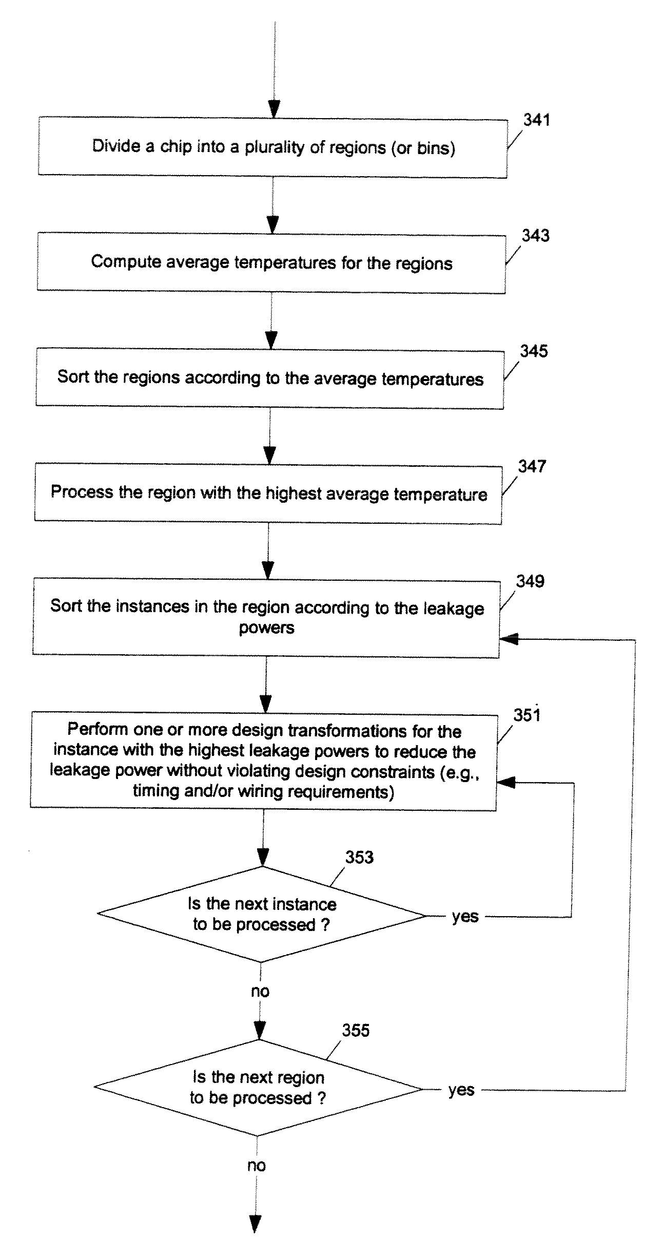
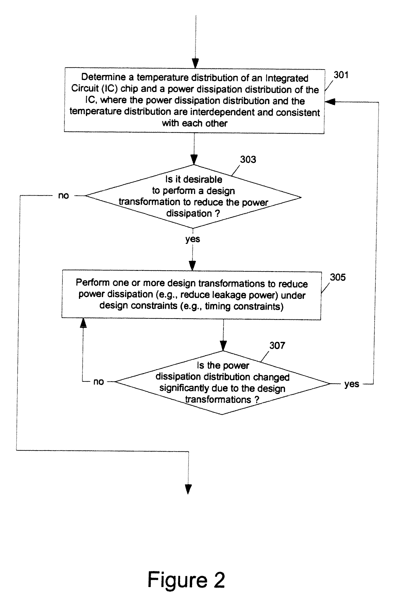
[0040]At least one embodiment of the present invention reduces the power dissipation and improves the timing of an integrated circuit to optimize the design. After computing the power dissipation in an original design, the temperature across the chip due to the heat generated is computed. Then, the components of the design are selectively transformed to reduce the power dissipation and to improve timing based on the temperature solution. For exampl...


PUM


Abstract

Methods and apparatuses for circuit design to reduce power usage, such as reducing temperature dependent power usage, and / or to improve timing, such as reducing temperature dependent delay or transition time. At least one embodiment of the present invention reduces the power dissipation and improves the timing of an integrated circuit to optimize the design. A thermal analysis is used to determine the temperature dependent power dissipation of a circuit and the temperature distribution of the circuit resulting from dissipating the heat created by the temperature dependent power dissipation. Then, the components of the design are selectively transformed to reduce the power dissipation and to improve timing based on the temperature solution. The transformation may include placement changes and netlist changes, such as the change of transistor threshold voltages for cells or for blocks of the circuit chip.

Description

[0001]This present application is a divisional of U.S. patent application Ser. No. 11 / 034,391, filed on Jan. 11, 2005.FIELD OF THE TECHNOLOGY[0002]The invention relates to automated circuit design, and more particularly to the automated transformation and optimization of a design of a circuit for improved timing and reduced power.BACKGROUND[0003]For the design of digital circuits (e.g., on the scale of Very Large Scale Integration (VLSI) technology), designers often employ computer-aided techniques. Standard languages such as Hardware Description Languages (HDLs) have been developed to describe digital circuits to aid in the design and simulation of complex digital circuits. Several hardware description languages, such as VHDL and Verilog, have evolved as industry standards. VHDL and Verilog are general-purpose hardware description languages that allow definition of a hardware model at the gate level, the register transfer level (RTL) or the behavioral level using abstract data type...

Claims


Application Information

Patent Timeline
Patent Type & Authority Applications(United States)
IPC IPC(8): G06F17/50
CPCG06F17/5036G06F17/50G06F2217/16G06F2111/10G06F30/367G06F30/00
Inventor RAHMAT, KHALIDMCELVAIN, KENNETH S.
Owner SYNOPSYS INC
Why Eureka
Try Eureka