Booster circuit

a technology of booster circuit and circuit, applied in the direction of power conversion system, dc-dc conversion, instruments, etc., can solve the problems of increase in layout area and decrease in boost efficiency, and achieve the effect of reducing layout area, improving easiness of design, and suppressing the increase in circuit area

Active Publication Date: 2008-07-17
PANASONIC SEMICON SOLUTIONS CO LTD
View PDF12 Cites 22 Cited by
  • Summary
  • Abstract
  • Description
  • Claims
  • Application Information

AI Technical Summary

Benefits of technology

[0036]According to the seventh aspect, the first well region and the second well region are caused to have the same potential, so that a single well region can be shared by an N-channel transistor and a P-channel transistor, resulting in a decrease in layout area.
[0037]According to the eighth aspect, an analog comparison circuit is provided for each of all stages, so that the boosting cells can be caused to be of uniform parasitic capacitance, thereby making it possible to improve easiness of design.
[0038]According to the ninth aspect, an analog comparison circuit is provided every arbitrary number of stages, so that an increase in circuit area can be suppressed while securing the margins of the breakdown voltages of the second well region and the first well reg

Problems solved by technology

Also, charges supplied by the clock signals CLK1 and CLK2 are used to charge and discharge the N well 908, disadvantageously resulting in a decrease in boost efficiency.
Also, since the source and the N well 908 of the

Method used


Image

  • Booster circuit
  • Booster circuit
  • Booster circuit

Examples


Embodiment Construction

[0068]Hereinafter, a booster circuit according to the present invention will be described, by way of examples, with reference to the accompanying drawings.

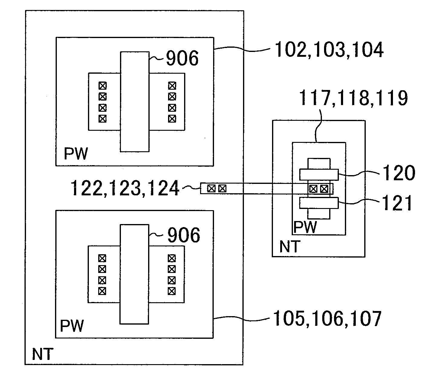
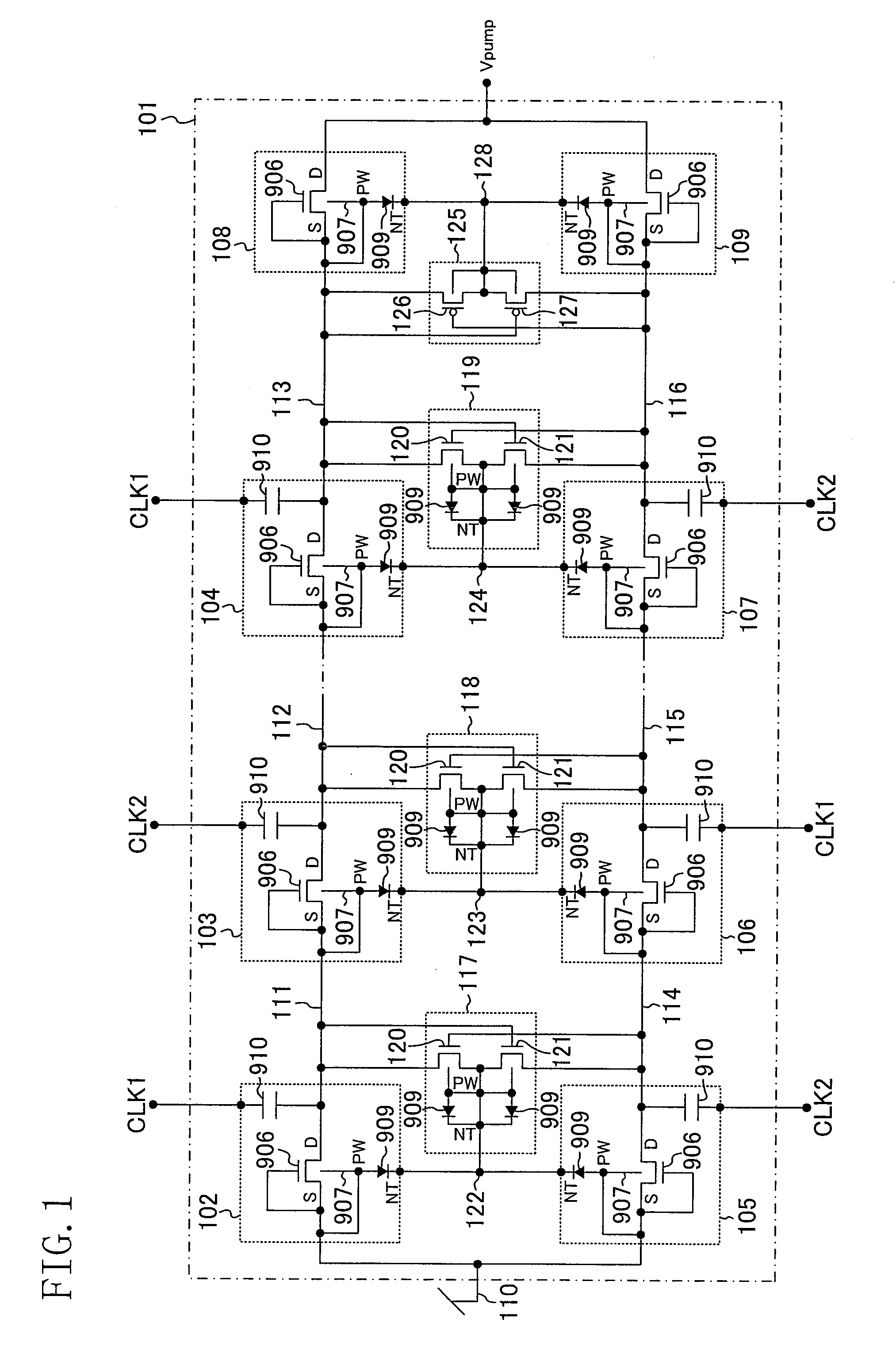
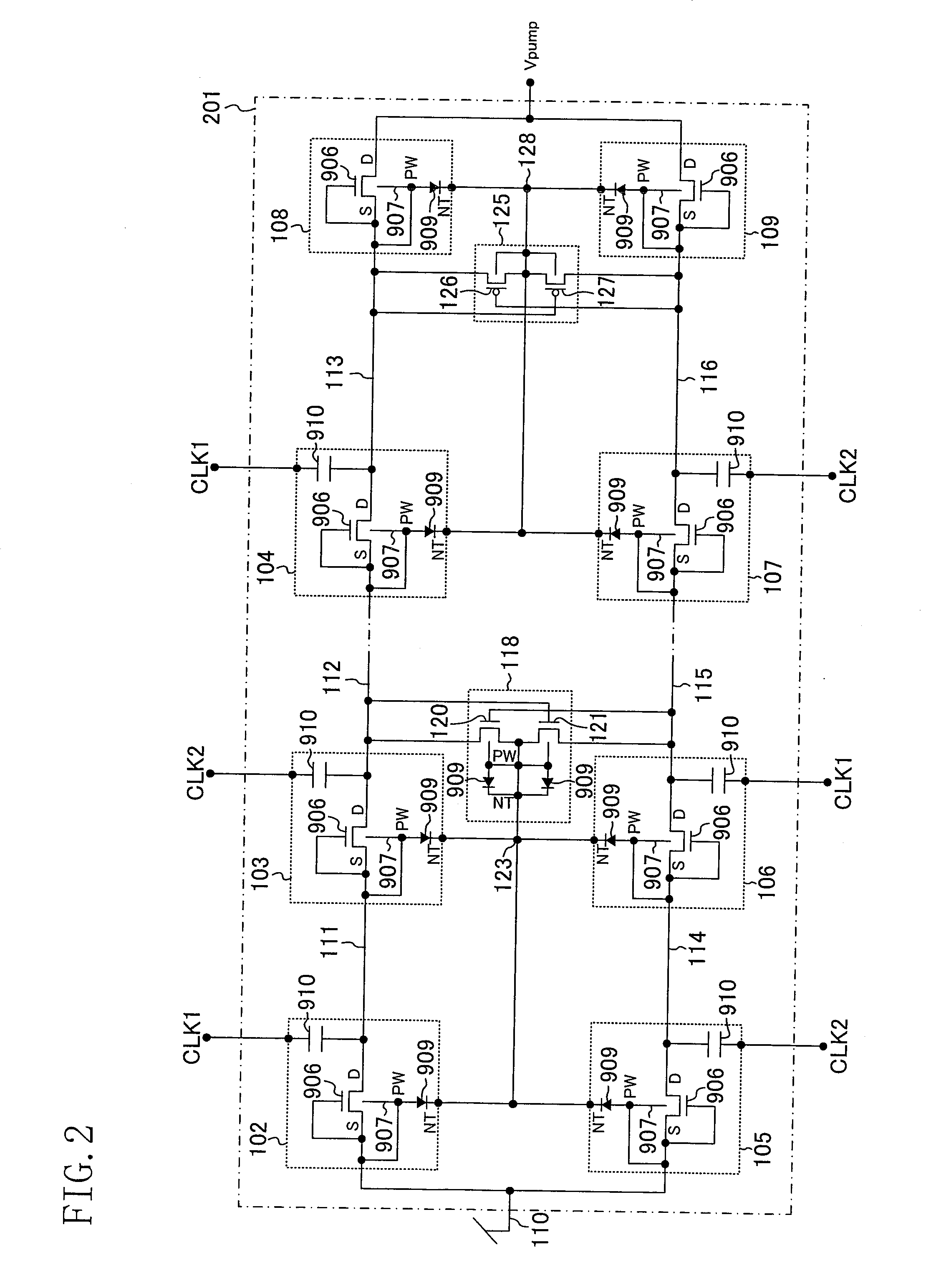
[0069]FIG. 1 shows an exemplary configuration of the booster circuit of the present invention. In FIG. 1, 101 indicates a two-parallel booster circuit which receives two-phase clock signals CLK1 and CLK2 and generates an output terminal voltage (boosted voltage) Vpump by a boosting operation. 102, 103, 104, 105, 106, and 107 indicate boosting cells which are arranged in a first line and a second line, where CLK1 is input to the odd-numbered stages on the first line and the even-numbered stages on the second line, and CLK2 is input to the even-numbered stages on the first line and the odd-numbered stages on the second line. 108 and 109 indicate backflow preventing circuits which prevent backflow of the boosted voltage Vpump. 110, 111, 112, 113, 114, 115, and 116 indicate I / O terminals of the boosting cells 102 to 107. 117, 118, and...


PUM


Abstract

A boosting circuit comprises a first boosting cell row and a second boosting cell row. The boosting circuit further comprises an analog comparison circuit for comparing the potential of boosting cells on the same stage, and selecting and outputting the lower or higher of the potentials. The potential of an N well is controlled using the output potential of the analog comparison circuit. Thereby, the amplitude of an N well potential can be suppressed, and a single N well region can be shared.

Description

BACKGROUND OF THE INVENTION[0001]1. Field of the Invention[0002]The present invention relates to a booster circuit employing a switching element having a triple-well structure.[0003]2. Description of the Related Art[0004]In recent years, flash memories, which are a type of non-volatile semiconductor memory devices, require data read and data write using a single power supply voltage or low power supply voltages, for which, therefore, a booster circuit for supplying a positive or negative boosted voltage is required on a chip when each operation is performed. Also, during CMOS processes, a power supply voltage generated by the booster circuit is used to improve characteristics of an analog circuit.[0005]Conventionally, there is a known booster circuit employing a triple-well structure switching element (U.S. Pat. Nos. 6,100,557, 6,121,821, and 7,102,422).[0006]FIG. 25 shows an exemplary conventional booster circuit. In FIG. 25, 901 indicates a booster circuit which receives two-phase...

Claims


Application Information

Patent Timeline
IPC IPC(8): G05F1/10
CPCG11C5/145H02M2003/075H02M3/073H02M3/075
Inventor YAMAHIRA, SEIJI
Owner PANASONIC SEMICON SOLUTIONS CO LTD
Why Eureka
Try Eureka