

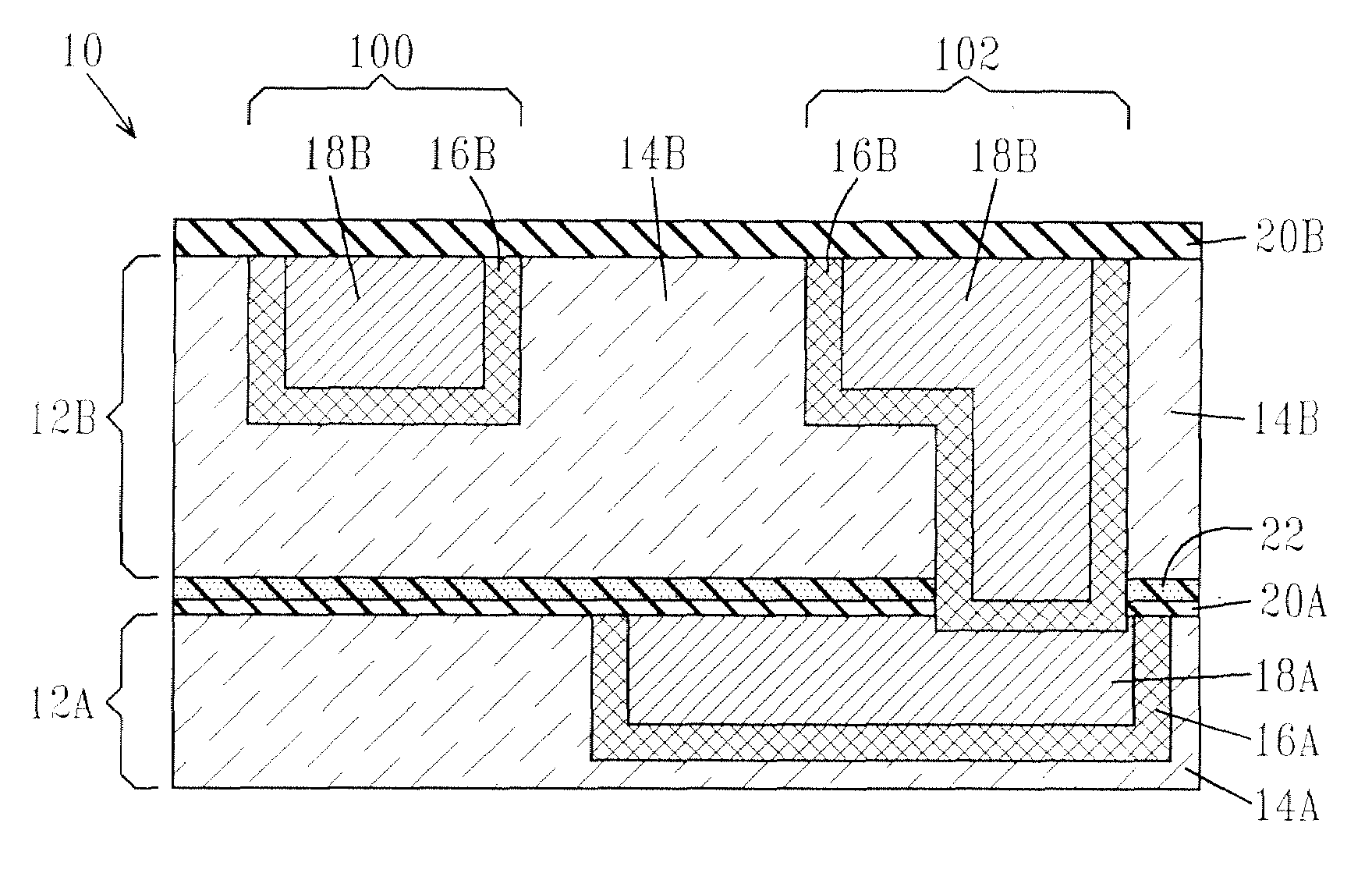
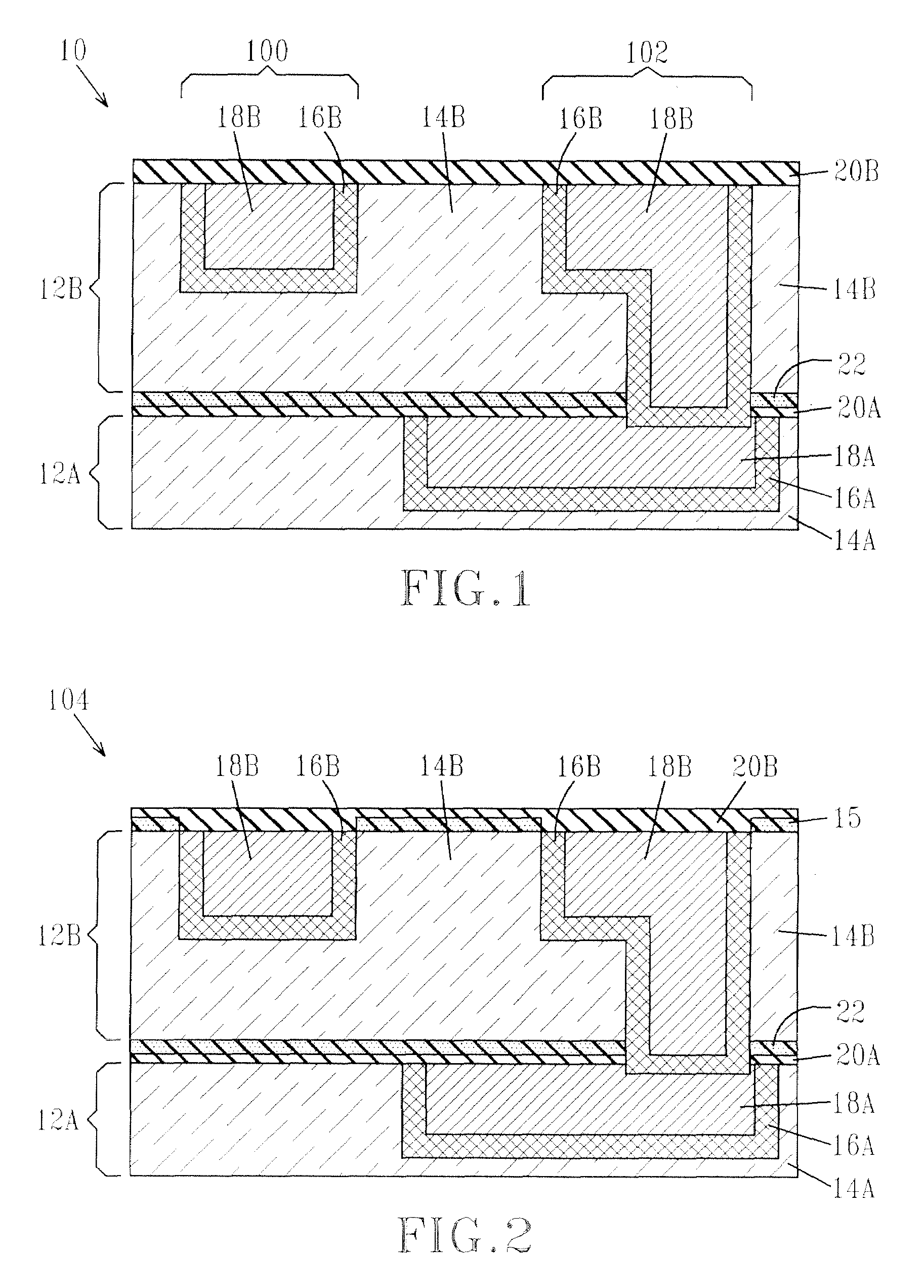
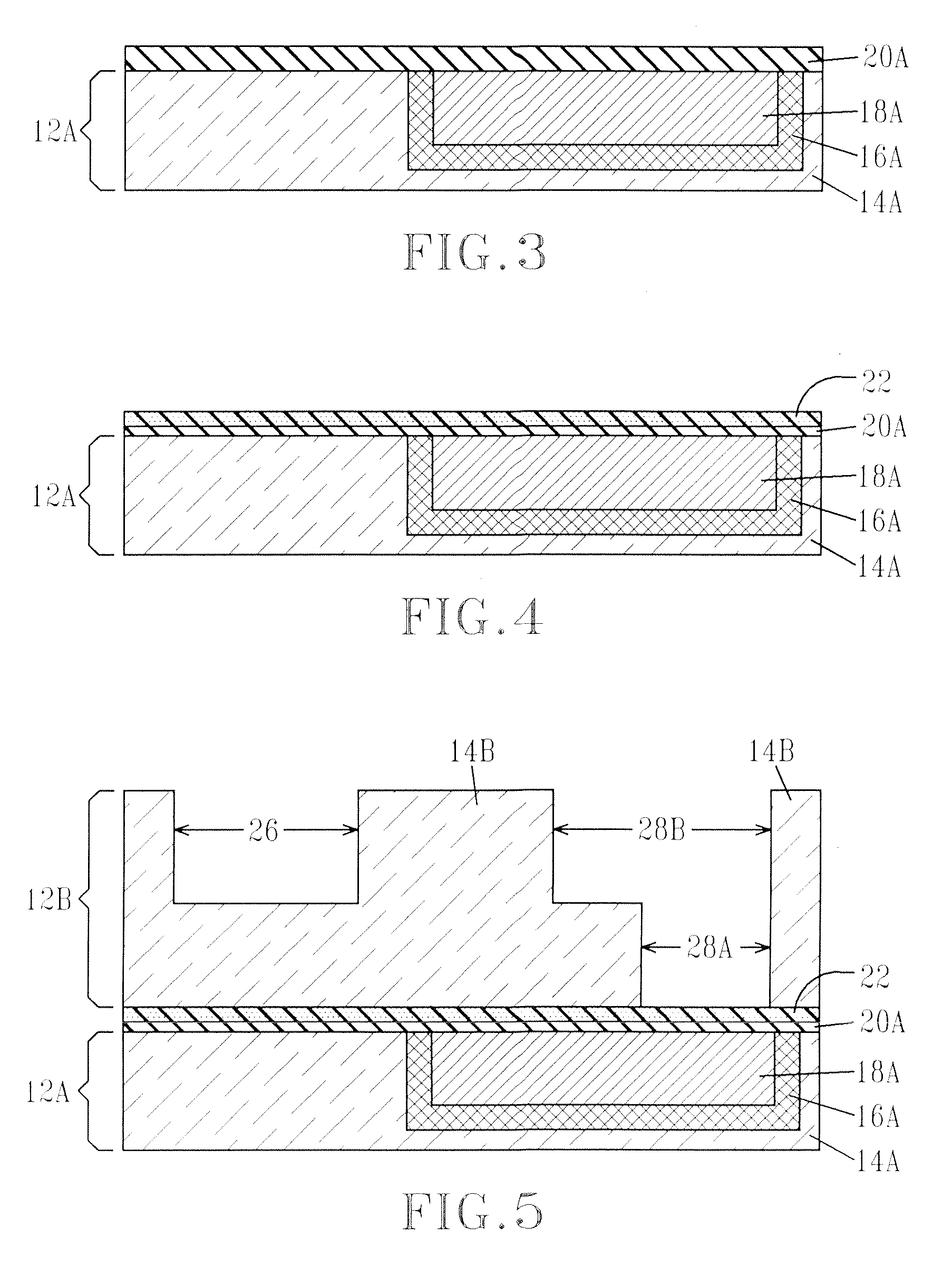
MECHANICALLY ROBUST METAL/LOW-k INTERCONNECTS
a low-k, mechanically robust technology, applied in the direction of semiconductor devices, semiconductor/solid-state device details, electrical apparatus, etc., can solve the problems of increasing signal delays in ulsi electronic devices, reliability failure during thermo-, delamination during fabrication and reliability failures, etc., to improve adhesion and improve adhesion
- Summary
- Abstract
- Description
- Claims
- Application Information
AI Technical Summary
Benefits of technology
Problems solved by technology
Method used
Image

Examples
example 1
Conventional; Not of the Invention
[0080]In this control example, a wafer containing an electronic structure having an upper layer of first dielectric with metal structures embedded in it was inserted in a plasma enhanced chemical vapor deposition (“PECVD”) reactor. The wafer was then heated to a temperature between room temperature and 350° C. In one example, Ar was flown into a 8″ the reactor at a rate of 30 sccm to achieve a pressure of 100 mTorr. A high frequency RF power source connected to the substrate holder was then turned on to about 60.0 W for 0.5 to 2 minutes. In a different example, the RF power generated was operated under bias control at a bias of −250 VDC. Without interrupting the plasma, the precursor mixture used for the deposition of the next dielectric film i.e., a SiCNH capping layer, was then flown into the reactor keeping the power and pressure unchanged until the flow was stabilized an then for an additional 5-15 seconds. The Ar flow was then shut off and the ...
example 2
NH3 Plasma
[0082]In this inventive example, a wafer containing an electronic structure having an upper layer of first dielectric with metal structures embedded in it was inserted in a plasma enhanced chemical vapor deposition (“PECVD”) reactor. The wafer was then heated to a temperature between room temperature and 350° C. In one example, Ar was flown into a 8″ the reactor at a rate of 30 seem to achieve a pressure of 100 mTorr. A high frequency RF power source connected to the substrate holder was then turned on to about 60.0 W for 0.5 to 2 minutes. In a different example, the RF power generated was operated under bias control at a bias of −250 VDC. Without interrupting the plasma, the precursor mixture used for the deposition of the next dielectric film (i.e., a SiCNH dielectric capping layer) was then flown into the reactor keeping the power and pressure unchanged until the flow was stabilized an then for an additional 5-15 seconds. The Ar flow was then shut off and the plasma con...
example 3
He Plasma
[0084]In this inventive example, a wafer containing an electronic structure having an upper layer of first dielectric with metal structures embedded in it was inserted in a plasma enhanced chemical vapor deposition (“PECVD”) reactor. The wafer was then heated to a temperature between room temperature and 350° C. In one example, Ar was flown into a 8″ the reactor at a rate of 30 sccm to achieve a pressure of 100 mTorr. A high frequency RF power source connected to the substrate holder was then turned on to about 60.0 W for 0.5 to 2 minutes. In a different example, the RF power generated was operated under bias control at a bias of −250 VDC. Without interrupting the plasma, the precursor mixture used for the deposition of the next dielectric film (i.e., a SiCNH dielectric capping layer) was then flown into the reactor keeping the power and pressure unchanged until the flow was stabilized an then for an additional 5-15 seconds. The Ar flow was then shut off and the plasma cond...
PUM
| Property | Measurement | Unit |
|---|---|---|
| dielectric constant | aaaaa | aaaaa |
| wavelength | aaaaa | aaaaa |
| temperature | aaaaa | aaaaa |
Abstract
Description
Claims
Application Information