Color filter and manufacturing method thereof, and electronic appliance having the color filter

a technology of color filter and manufacturing method, which is applied in the direction of photomechanical treatment originals, instruments, nuclear engineering, etc., can solve the problems of generating defects, troublesome correction work, and inefficient conventional correction method using laser beams, so as to improve the yield of color filters

Inactive Publication Date: 2008-07-31
SEMICON ENERGY LAB CO LTD
View PDF7 Cites 12 Cited by
  • Summary
  • Abstract
  • Description
  • Claims
  • Application Information

AI Technical Summary

Benefits of technology

[0022]According to the present invention, the defect resulting from the color mixing of the color filter materials in the adjacent pixel regions can be corrected easily, and a yield of the color filter is improved.

Problems solved by technology

However, even when the above measures are applied, color mixing of the color filter materials occurs in some cases, which leads to generation of a defect.
A conventional correcting method with the use of a laser beam is extremely inefficient because all the color filter materials in the pixel where a defect occurs are removed by irradiation with a laser beam, and a color filter material needs to be filled again in the pixel where all the color filter materials are removed.
Further, in a case of filling again the pixel where all the color filter materials are removed with the color filter material, each pixel is manually filled with the color filter material; therefore, there is a problem in that correcting work is very troublesome.

Method used


Image

  • Color filter and manufacturing method thereof, and electronic appliance having the color filter
  • Color filter and manufacturing method thereof, and electronic appliance having the color filter
  • Color filter and manufacturing method thereof, and electronic appliance having the color filter

Examples


embodiment mode 1

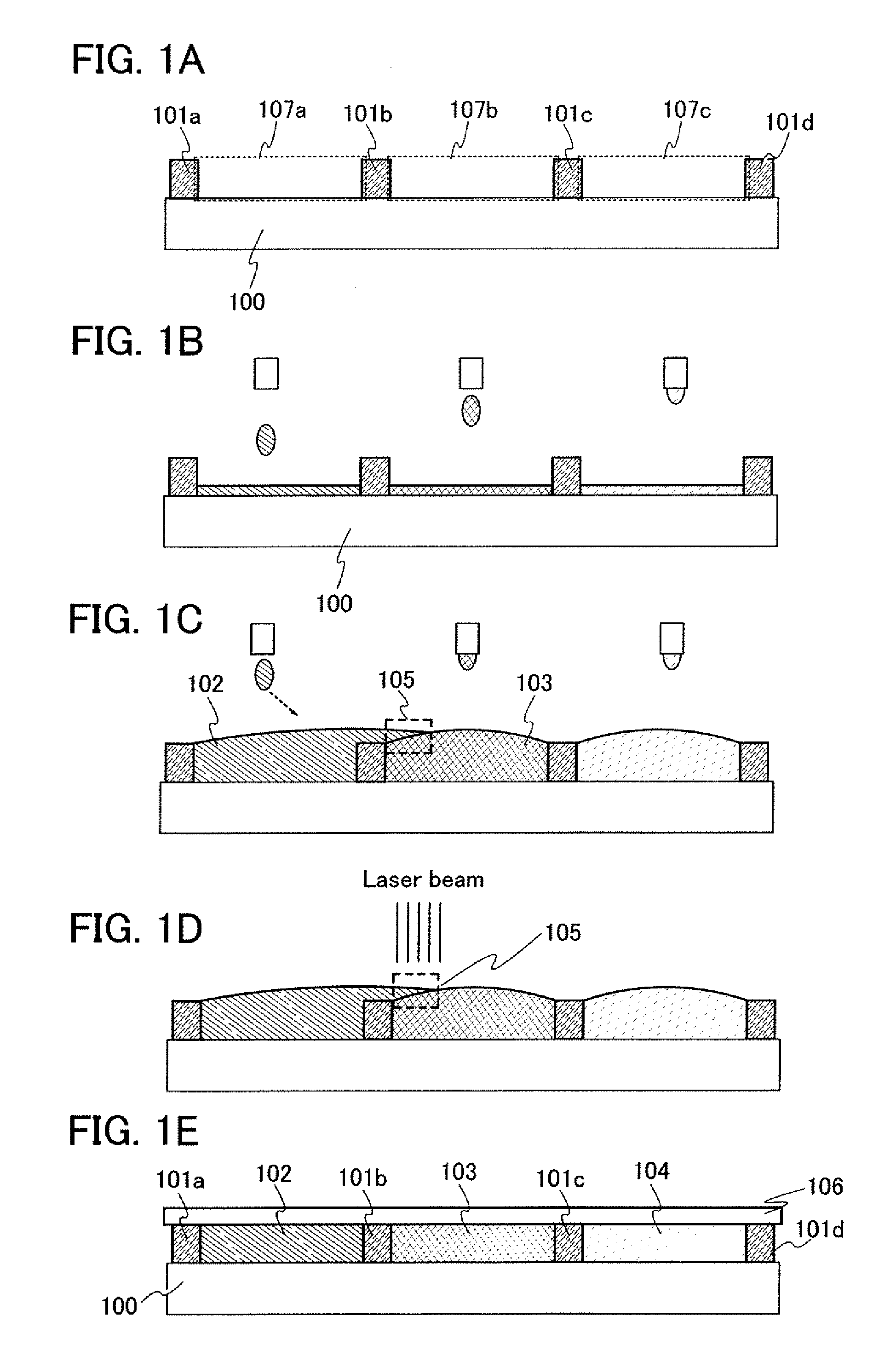
[0035]This embodiment mode will describe a color filter which is manufactured using a manufacturing method of the present invention.

[0036]First, a structure of the color filter in accordance with this embodiment mode is described. The color filter in this embodiment mode includes partition walls (black matrixes) 101a to 101d which are formed over a light-transmitting substrate 100, a colored layer (R) 102, a colored layer (G) 103, a colored layer (B) 104 as shown in FIG. 1E. Further, the color filter also includes a resin layer 106 which is formed over the partition walls 101a to 101d, the colored layer (R) 102, the colored layer (G) 103 and the colored layer (B) 104.

[0037]Hereinafter, a method for manufacturing the color filter in accordance with this embodiment mode is described with reference to FIGS. 1A to 1E. First, the partition walls 101a to 101d are formed over the light-transmitting substrate 100 (see FIG. 1A), so that depressed portions to which color filter materials are ...

embodiment mode 2

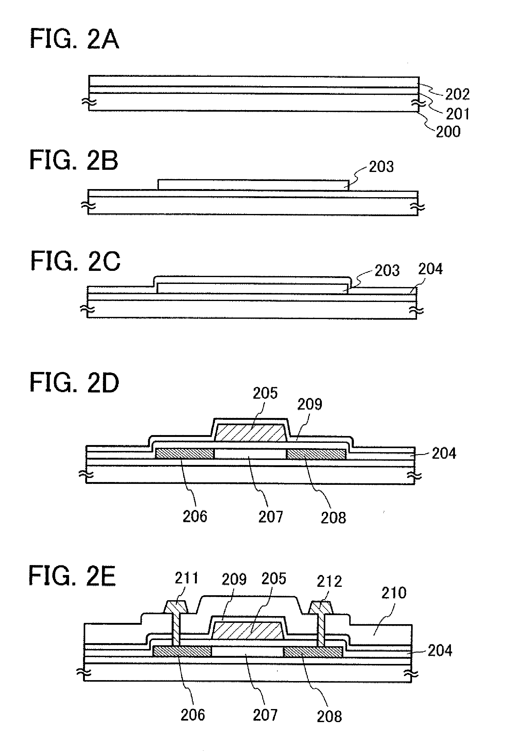
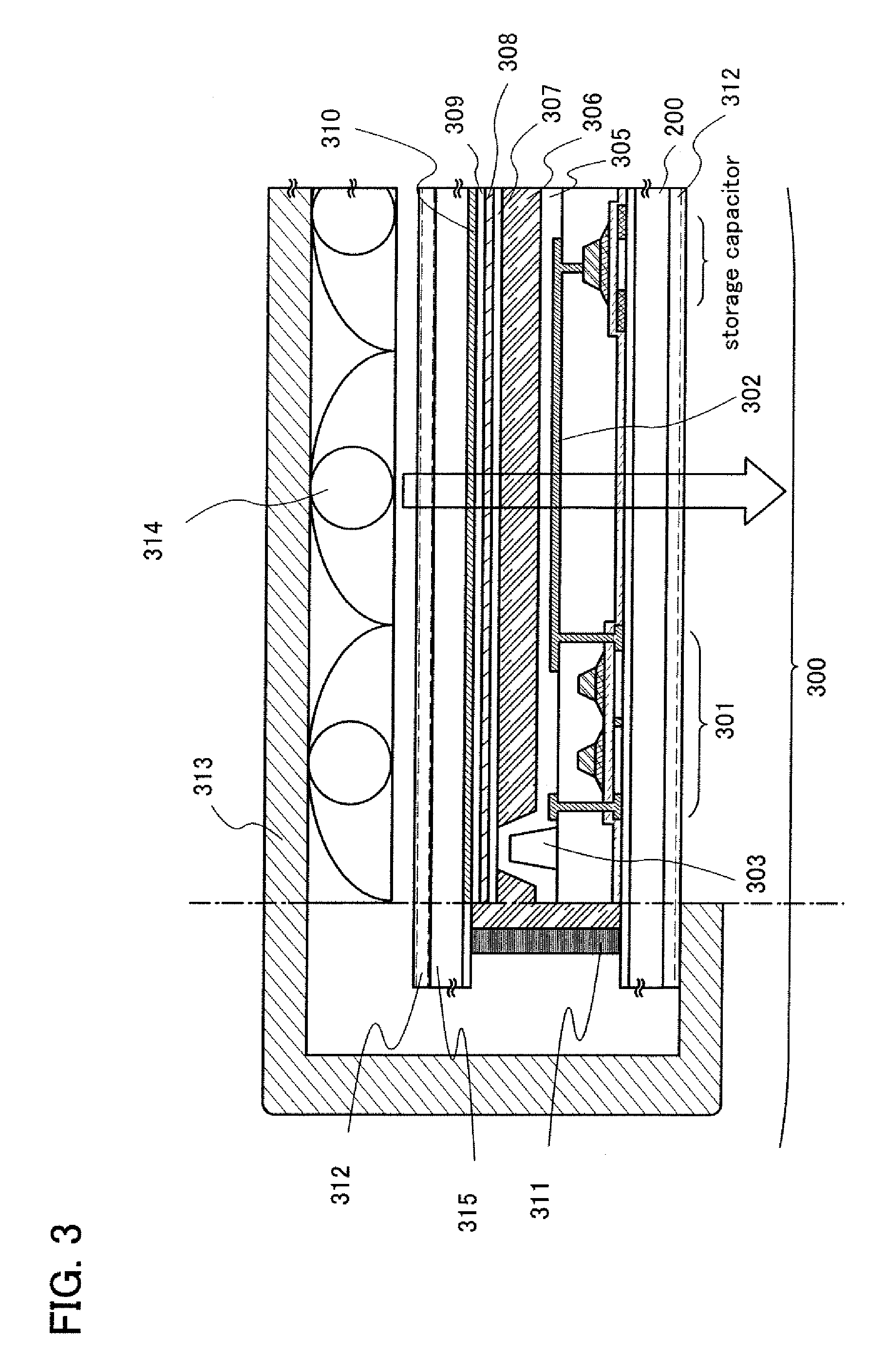
[0059]This embodiment mode shows a manufacturing example of an active matrix liquid crystal display device using a color filter (see FIG. 3).

[0060]First, a pixel portion 300 is formed by forming a semiconductor layer and a TFT 301 having the semiconductor layer as its active layer, and the like over a substrate 200. A procedure for manufacturing a TFT is hereinafter described simply with reference to FIGS. 2A to 2E.

[0061]In FIG. 2A, a reference numeral 200 denotes a substrate having an insulating surface; 201, an base insulating film as a blocking layer; and 202, a semiconductor film having a crystalline structure.

[0062]In FIG. 2A, the substrate 200 may be a glass substrate, a quartz substrate, a ceramic substrate, or the like. Further, a silicon substrate, a metal substrate, or a stainless steel substrate having an insulating film formed over its surface may be used. Furthermore, a plastic substrate having heat resistance which can withstand process temperature in this step may als...

embodiment mode 3

[0086]This embodiment mode will describe a method for manufacturing a light-emitting device having an EL element (FIGS. 4A and 4B), which is also referred to as an organic EL display or an organic light-emitting diode, with the use of the color filter of the present invention. Note that FIG. 4B is a top view of the light-emitting device in this embodiment mode. FIG. 4A is a cross sectional view taken along a dashed line A-B of FIG. 4B.

[0087]An EL element having a layer including an organic compound as a light-emitting layer has a structure in which the layer including an organic compound (hereinafter referred to as an EL layer) is interposed between an anode and a cathode. By application of an electric field to the anode and the cathode, luminescence (electro luminescence) is generated from the EL layer Light emitted from the EL element includes light generated when a singlet-excited molecules relaxes to a ground state (fluorescence) and light generated when a molecules in the tripl...


PUM

PropertyMeasurementUnit
wavelength regionaaaaaaaaaa

Abstract

The present invention provides a method for manufacturing a color filter to facilitate the correction of the defect which is caused by the undesirable mixing of plural color filter materials with different color. Further, the present invention provides a color filter manufactured by the present method for manufacturing the color filter and also a semiconductor device using the color filter manufactured by the present method. In the manufacturing method of the present invention, the color-mixed portion which is undesirably formed during the production of the color-filter by using a plurality of color filter materials is irradiated with a laser beam which is different in transmissivity to each color filter material. This method allows the color filter material which is necessary to remain and the color filter material which is unnecessary to be selectively removed.

Description

BACKGROUND OF THE INVENTION[0001]1. Field of the Invention[0002]The present invention relates to a method for manufacturing a color filter which is used for a display panel. Further, the present invention relates to a color filter which is manufactured by the above-described manufacturing method and an electronic appliance having the color filter.[0003]2. Description of the Related Art[0004]In recent years, demand of a display, especially, a color display has tended to increase due to the development of personal computers and the like. In the color display such as a liquid crystal display panel, the color filter for full color display is formed on a counter substrate. Polarizing plates are provided as a light shutter to an element substrate and the counter substrate, so that a full color image is displayed.[0005]Here, the color filter of the liquid crystal display panel has colored layers of R (Red), G (Green) and B (Blue) and light-shielding partition walls (black matrixes) which a...

Claims


Application Information

Patent Timeline
Patent Type & Authority Applications(United States)
IPC IPC(8): G02F1/13
CPCY10S430/146G02F1/133516G02B5/20
Inventor FUKAI, SHUJIKUNIZAKI, KANAKO
Owner SEMICON ENERGY LAB CO LTD
Why Eureka
Try Eureka