Fabrication method of semiconductor package

a technology of semiconductor packaging and fabrication method, which is applied in the direction of semiconductor devices, semiconductor/solid-state device details, electrical devices, etc., can solve the problems of reducing yield, increasing fabrication cost, and tin-plating process not meeting unleaded demand, so as to reduce fabrication cost and increase yield

Inactive Publication Date: 2008-07-31
TAIWAN SOLUTIONS SYST CORP
View PDF2 Cites 14 Cited by
  • Summary
  • Abstract
  • Description
  • Claims
  • Application Information

AI Technical Summary

Benefits of technology

[0006]In order to solve the foregoing problems, one object of this invention is to provide a fabrication method of a semiconductor package without using any tape, so that the conve

Problems solved by technology

Besides, the processes of mounting the tape, removing the tape and purging the viscose will increase the fabrication cost and decrease the yield.
But the tin-plating process does not satisfy the unleaded demand of the restriction of the use of certain hazardous substrate in E

Method used


Image

  • Fabrication method of semiconductor package
  • Fabrication method of semiconductor package
  • Fabrication method of semiconductor package

Examples


Embodiment Construction

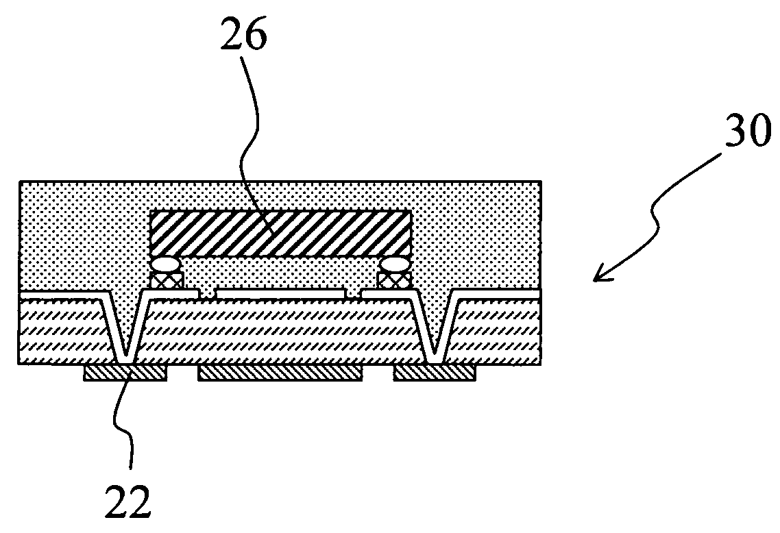
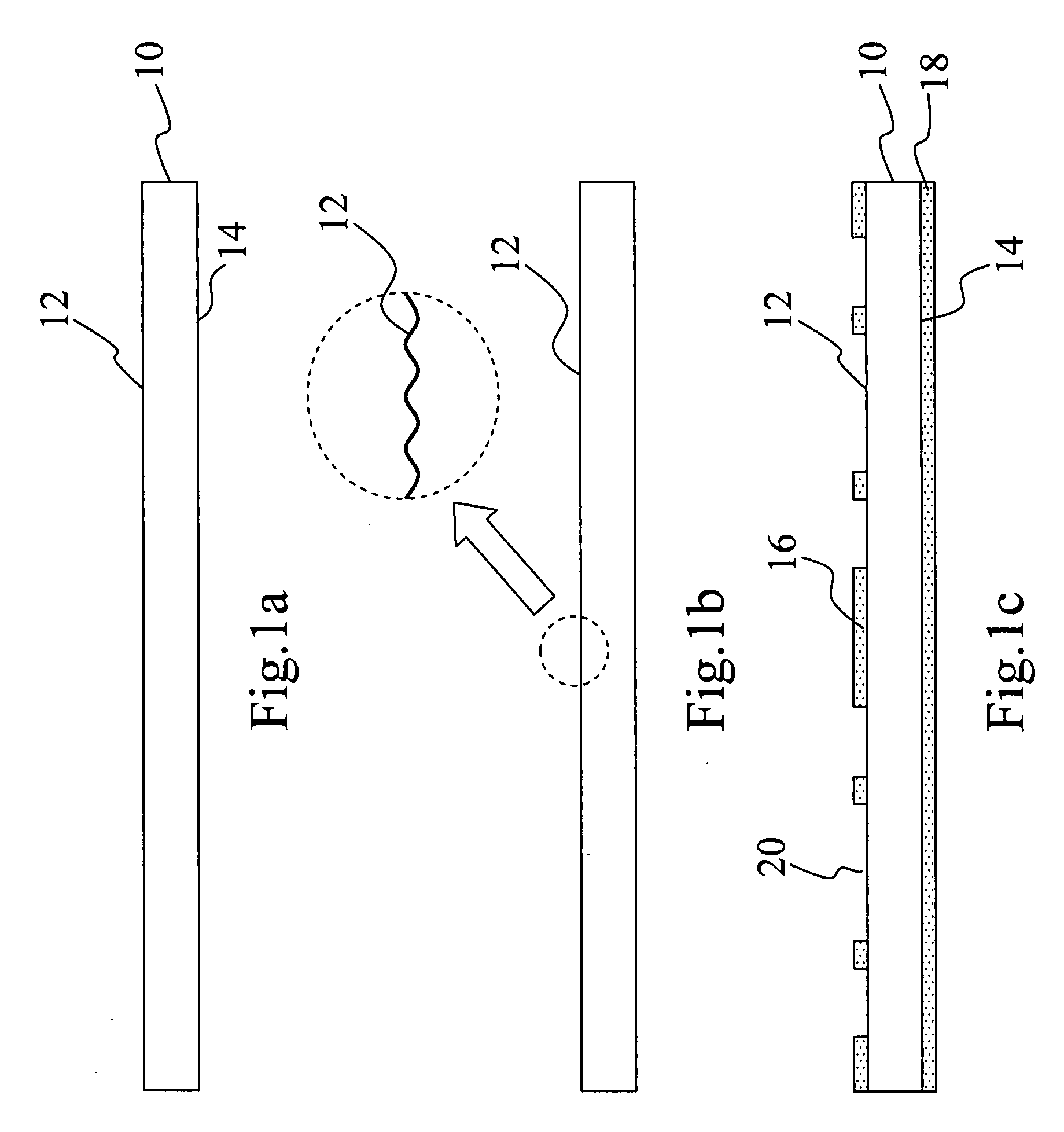
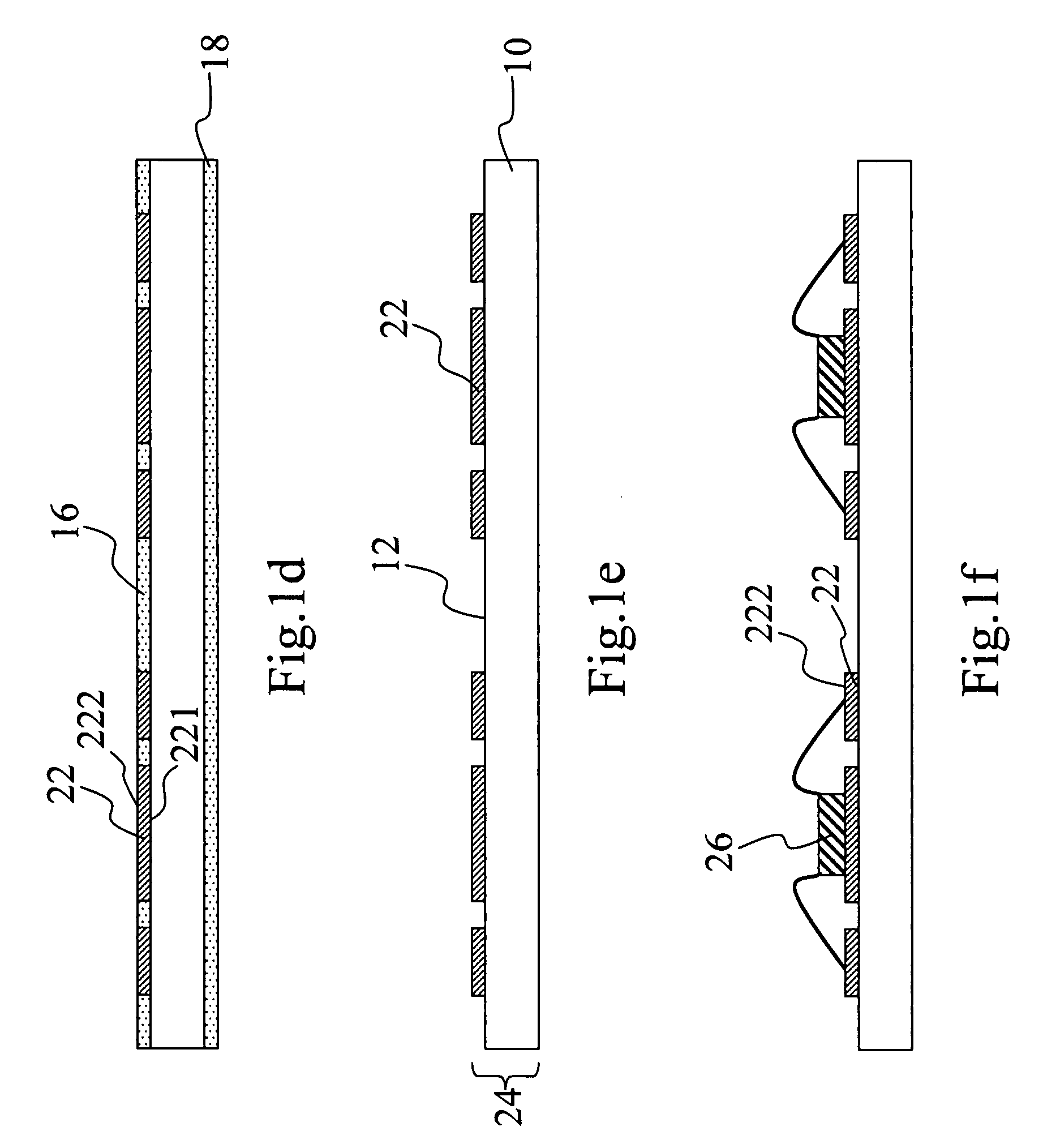
[0021]FIG. 1a to FIG. 1i are cross-sectional diagrams illustrating the fabrication method of a semiconductor package in accordance with an embodiment of the present invention. First, as shown in FIG. 1a, a carrier 10 is provided. The carrier 10 has a first surface 12 and a second surface 14, and the material of the carrier 10 is metal. A special surface treatment is performed to the first surface 12 to form the rough structure or the reticular structure on the first surface 12, as shown in FIG. 1b, which includes a partial enlarged diagram of the surface 12 in FIG. 1a. Please refer to FIG. 1c, a patterned insulating layer 16 covers the first surface 12 and an insulating layer 18 covers the second surface 14. A plurality of the openings 20 are formed on the patterned insulating layer 16 according to the chip-mounted positions and the circuit design, to expose portions of the first surface 12. Next, a plurality of metal-stack layers 22 are respectively disposed in the plurality of the...


PUM


Abstract

A fabrication method of a semiconductor package is applied to fabricate the package with the lead frame. The fabrication method includes: performing a surface treatment on a carrier; electroplating a plurality of metal-stacked layers on the surface of the carrier, wherein the top of the metal-stacked layer is a bonding surface and the bottom of the metal-stacked layer is a welding surface; performing a chip bonding step; forming a molding compound on the carrier; removing the carrier and performing a dicing step to form a plurality of semiconductor packages. The fabrication method of a semiconductor package also includes that forming a plurality of cavities on the carrier surface, electroplating the metal-stacked layer on the cavities, and then performing the chip bonding step, forming the molding compound on the carrier; remove the carrier and performing the dicing step. Using the foregoing steps can prevent the overflow situation without using any tape.

Description

BACKGROUND OF THE INVENTION[0001]1. Field of the Invention[0002]The present invention relates to a fabrication method of a semiconductor package, and, more especially, to the fabrication method of the semiconductor package with a lead frame structure.[0003]2. Background of the Related Art[0004]In the traditional package processes, a tape is required to arrange on the SMT mounting surface of the lead frame before proceeding the molding process, in order to prevent the molding flow over to the SMT pads and affect the follow-up manufacturing process. However, the tape will remain the viscose on the SMT mounting surface to pollute the SMT pads. Besides, the processes of mounting the tape, removing the tape and purging the viscose will increase the fabrication cost and decrease the yield. Therefore, how to prevent the molding flow over to the SMT mounting surface without using any taps is a characteristic of the present invention.[0005]On the other hand, during the traditional package pr...

Claims


Application Information

Patent Timeline
IPC IPC(8): H01L21/60
CPCH01L21/568H01L2224/48247H01L23/3107H01L23/3121H01L24/16H01L24/48H01L24/81H01L24/85H01L24/97H01L2221/68345H01L2224/16H01L2224/48091H01L2224/48227H01L2224/81801H01L2224/85411H01L2224/85439H01L2224/85444H01L2224/85447H01L2224/97H01L2924/01029H01L2924/01046H01L2924/01047H01L2924/01078H01L2924/01079H01L2924/01082H01L21/6835H01L2224/16245H01L2924/01033H01L2224/85H01L2924/00014H01L2224/81H01L2924/181H01L2924/00011H01L2924/00012H01L2224/0401H01L2224/45099H01L2224/45015H01L2924/207
Inventor LIN, CHI CHIHSUN, BOWANG, HUNG JENTSENG, JEN FENG
Owner TAIWAN SOLUTIONS SYST CORP
Why Eureka
Try Eureka