Embedded time domain analyzer for high speed circuits

a time domain analyzer and high-speed circuit technology, applied in the direction of pulse technique, pulse characteristics measurement, transmission monitoring, etc., can solve the problems of circuitry for testing adding additional problems, not improving the functions of primary circuits, and not being more robust to process or environmental parameters variations

Inactive Publication Date: 2008-07-31
MCGILL UNIV
View PDF9 Cites 30 Cited by
  • Summary
  • Abstract
  • Description
  • Claims
  • Application Information

AI Technical Summary

Problems solved by technology

Implementing DFT into an IC typically results in add-on test circuitry, which does not improve the primary circuit functions.
It does not make a circuit faster, it does not reduce the power consumption, and it does not make it more robust to variations of process or environmental parameters.
Even worse, the circuitry for testing adds additional problems.
Chip complexity increases, and a particularly elegant circuit solution is often questionable after test circuitry has “ruined” the layout.
DFT strategies are not merely an add-on module to an existing, and working, circuit solution but dominantly shape the semiconductor circuit solution, by for example determining the module boundaries, bring limitations and restrictions to the freedom of the analog designer and of the circuit implementation, and require additional circuitry which increases the die area, therefore increasing the die manufacturing costs and increasing the probability of faults in the chip.
However, with digital circuits routinely operating at 10 Gb / s and above in telecommunications and developments extending to 40 Gb / s and 100 Gb / s, the line between digital and analog signals is increasingly blurring.
Hence, the original differentiations between analog and digital test equipment are disappearing and circuit designs at these high speeds and operating frequencies becoming more synergistic in building blocks, semiconductor technology and testing requirements.
However, common to such prior art comparator based approaches the simplicity was traded off against increased test time, due to requiring the reference voltage to be swept over all possible levels and settle for each “measurement”.
Hardware complexity is decreased at the expense of increased test time due to the dual-loop system.
Importantly the under sampling approach does not allow the capture of single events, such as occur with one-off error events within ICs or systems measuring nuclear interactions, or even those operating in safety critical or high reliability situations where on-line functional verification is required.
In these instances there is no repetition, and the prior art solutions could only provide a solution with the further integration of a recirculating delay line capable of providing the multiple repetitions of the signal being characterized.

Method used


Image

  • Embedded time domain analyzer for high speed circuits
  • Embedded time domain analyzer for high speed circuits
  • Embedded time domain analyzer for high speed circuits

Examples


Embodiment Construction

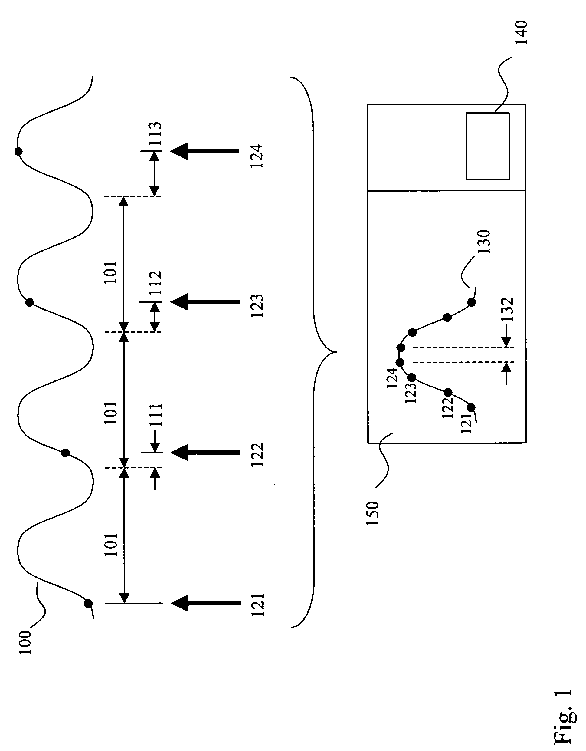
[0074]Referring to FIG. 1, illustrated schematically is the prior art approach of under-sampling to characterize a high-speed signal. Shown is a repetitive waveform 100 having a period ΔT 101, which is sampled with a sampling instrument at initial time point 121 and subsequent time points 122, 123, and 124. The subsequent time points 122, 123 and 124 are delayed sequentially relative to each preceding time point 121, 122, and 123 respectively by δT. As a result, the second sampling point 122 is delayed by a delay 111 equal to δT, the third sampling point 123 is delayed by an overall delay 112 of 2δT, and the fourth sampling point 124 is delayed by an overall delay 113 of 3δT relative to the repeating waveform 100 of period ΔT 101.

[0075]The resulting samples 121 through 124 are then processed by a processor 140, which takes the sampled signals from the sampling head (not shown for clarity) and drives an oscilloscope display 150. This results in each of the sampled points 121 through ...


PUM


Abstract

A method of providing an on-chip high-speed time domain digital analyzer for the characterization and analysis of signals within an integrated circuit is provided. The method involves processing the signal being characterized / analyzed in the digital domain irrespective of it's starting format. The approach performs a voltage-to-time conversion using predetermined voltage thresholds, applying a time amplification to the digital time information, measuring the amplified time difference between events and converting the amplified time difference as required by the characterization / analysis. The method allows the capture of very high-speed signals with high resolution without the requirements of complex and high-speed electronics. As such the on-chip high-speed time domain digital analyzer can function as an oscilloscope, pulse width analyzer, rise time analyzer and even logic analyzer. Further the method allows the capture and analysis of single and non-repetitive signal events unlike prior art approaches to time domain oscilloscopes.

Description

FIELD OF THE INVENTION[0001]The invention relates to performing time domain measurements of electronic circuits, and particularly to embedding of time domain analyzer functions into high-speed integrated circuits.BACKGROUND OF THE INVENTION[0002]Design for Test (DFT) has gone in recent years from a somewhat beneficial feature to a necessity within integrated circuits. Originally focused on digital circuits with the inclusion of circuit elements for Built-In Self-Test (BIST), and subsequently expanding to Built-In Test Equipment (BITE), the DFT methodology has now penetrated all areas of electronics and IC design, but is especially important with increasing operational speeds and increased integration in analog and mixed signal circuits where demands for performance, reliability, and defectivity are increasing whilst customer continually demand decreasing costs and guaranteed supply.[0003]The motivations to employ DFT strategies in IC design are not always obvious at the first glance...

Claims


Application Information

Patent Timeline
Patent Type & Authority Applications(United States)
IPC IPC(8): G01R29/02
CPCG01R31/3167G01R31/31726G01R31/31725
Inventor ROBERTS, GORDON W.SAFI-HARAB, MOUNAOULMANE, MOURAD
Owner MCGILL UNIV
Why Eureka
Try Eureka