Simple Bus Buffer

Active Publication Date: 2008-07-31
HENDON SEMICON
View PDF20 Cites 15 Cited by
  • Summary
  • Abstract
  • Description
  • Claims
  • Application Information

AI Technical Summary

Benefits of technology

[0065]Therefore in this invention our solution to the glitch problem on the CLK line is to make the CLK unidirectional, and to forego the luxury of full bi-directional operation, which makes a glitch free buffer design so difficult.
[0066]By doing this the lack of bi-directional capability on the CLK line prevents the use of pulse stretching by the slave device on the output side of the bus. Where a slave device on the output side of the buffer is unable to operate as quickly as the master, which up to this time has been generating the clock signal, clock stretching allows the slave to take over by pulling the CLK line low on the other side of the buffer in order to stretch the clock pulse to a pulse length more appropriate to its required speed of operation. It is therefore a limitation on the application of a buffer as described in this invention that applications using clock stretching are unable to use this buffer. However it should be able to be used in applications not needing pulse stretching. As slave devices needing clock stretching can be identified, these clock stretching stations may be able

Problems solved by technology

In many cases the full bi-directional capability is not used, and presents unnecessary complexity to fully meet all aspects of the I2C system standards, even when these features are not used or needed in many specific applications.
If the bus capacitance is increased then the maximum possible speed of the bus is limited, and the slower rise times on the bus start to cause difficulties.
This presents a challenge to design an efficient printed circuit layout with so many interconnections on the circuit board.
Much of the complexity is because it requires parallel bus pins on each IC to accommodate all of these interconnections.
But a display needs no reverse signal path, and could use a buffer which does not offer the full bi-directional capability.
Most of these circuits have problems which may be associated with latching, be only conditionally stable, or present glitches.
The usual limitation presented by such circuits is that they are unable to reverse their direction of signal flow when active, generating a glitch that can upset the bus I2C function.
Oscillation in such a loop then becomes another possible problem.
A more subtle problem arises because the I2C Bus protocol has been defined so that two or more ICs may t

Method used


Image

  • Simple Bus Buffer
  • Simple Bus Buffer
  • Simple Bus Buffer

Examples


Embodiment Construction

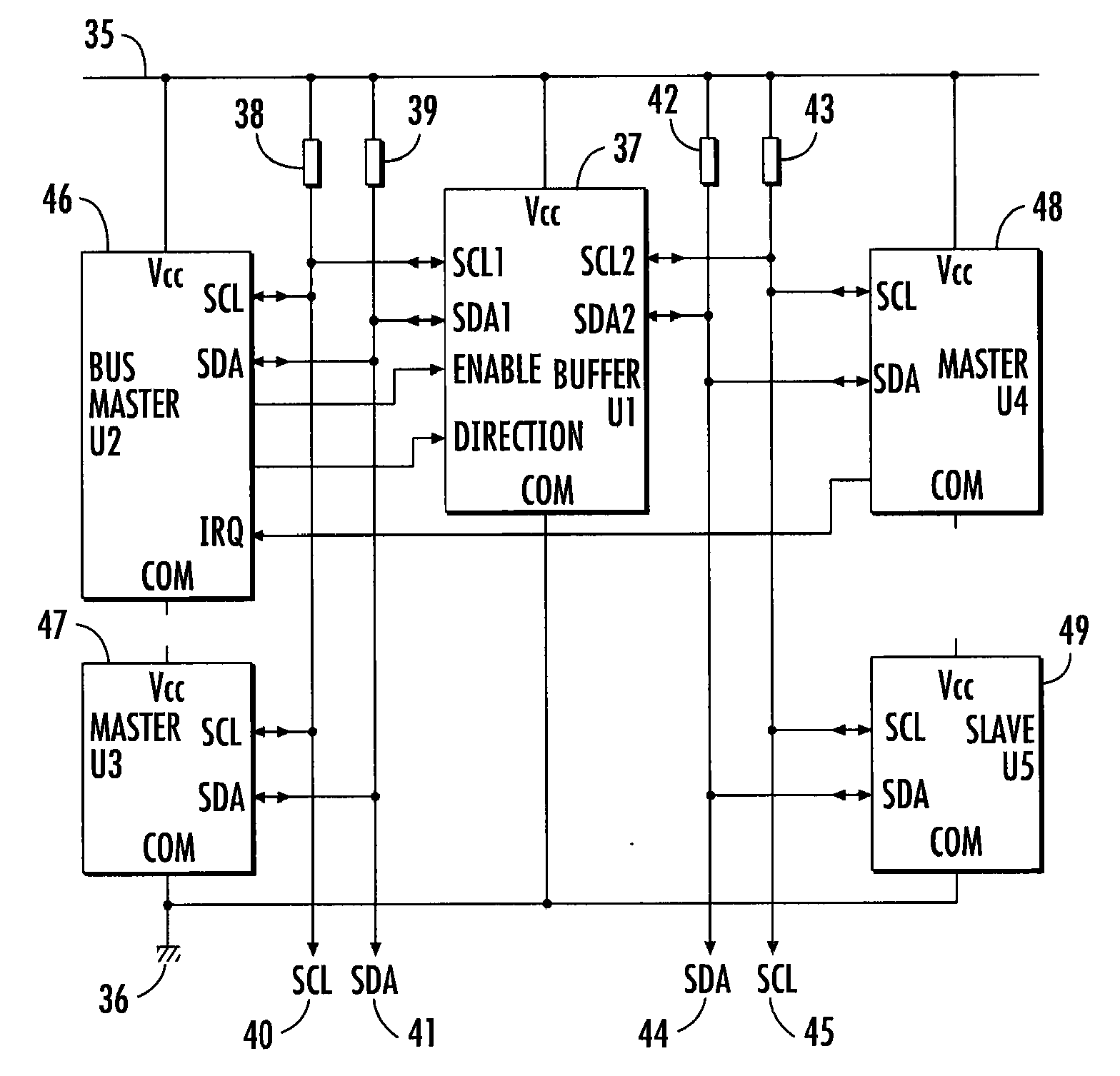
[0077]The basic structure of the buffer is shown in FIG. 1. The two buffer circuits comprising the upper data buffer are symmetrical, with an output signal that follows the input voltage offering bi-directional buffer action. The lower clock buffer is active in either the forward, or reverse direction, with the signal path direction controlled by a direction input. It also has an enable function applied to both sections of the buffer. That is to the forward or reverse path for the SCL clock signal and to the bi-directional SDA data path contained in the buffer IC.

[0078]The integrated circuit 10 in this example, has 8 connecting pins. There is the positive supply 11 (VCC), the common negative power supply connection 12 (COM or VEE), the direction control pin 13 (Direction) and the enable control pin 14 (Enable), and the inputs and outputs of the two buffer sections.

[0079]The inputs to the buffer are all schmitt inputs to enable it to be used with slowly changing input signals. A resu...


PUM


Abstract

A bus buffer can include a data buffer and a clock signal buffer. The data buffer for can include two symmetrical buffer circuits with an output signal that can follow the input voltage to provide bi-directional buffer action for a data path of the bus buffer. The clock buffer can operate in a forward or reverse direction, where the signal direction for the clock signal path in the bus buffer can be controlled with a direction input. The bus buffer can also include an enable circuit for enabling the data path and the clock signal path.

Description

TECHNICAL FIELD[0001]This invention relates to a buffer for a bi-directional signal transmission system by which a digital signal can be transmitted in both directions.BACKGROUND ART[0002]A number of two wire bi-directional signal transmission systems have been extensively used. One such system is the Inter Integrated Circuit Bus system (I2C Bus system), disclosed in the Philips Data Handbook IC12a, 1989, and “The I2C Bus and how to use it (including specifications)” 1995 Philips Semiconductors.[0003]The I2C Bus system is a serial bus system between individual integrated circuits, or stations, that are interconnected through a bi-directional two wire transmission channel. Of the two wires, one carries a clock signal, and the other the data, with a predetermined communication protocol. Depending on the particular function within the system, an individual station can act as the transmitter, or as a receiver. In many cases the full bi-directional capability is not used, and presents un...

Claims


Application Information

Patent Timeline
IPC IPC(8): G06F3/00
CPCG06F13/4077
Inventor BOURNE, PAULMURFETT, DAVIDTRACY, PHILIPMALCOLM, KAYMARK, POTTERJOHN, CRAWFORD
Owner HENDON SEMICON
Why Eureka
Try Eureka