
Press-Fit Terminal, a Method for Manufacturing the Same, and a Structure of Connection Between a Press-Fit Terminal and a Circuit Board

Inactive Publication Date: 2008-08-07
AUTONETWORKS TECH LTD +2
View PDF0 Cites 47 Cited by
  • Summary
  • Abstract
  • Description
  • Claims
  • Application Information

AI Technical Summary

Benefits of technology

[0026]According to the press-fit terminal described in claim 1, the press-fit connecting part has a layer in which the unalloyed Sn having a depth of a few to 50 nm from an outer surface of the layer and the Sn based alloy are mixed. Hardness of the Sn based alloy layer is made considerably higher than that of Cu plating provided to an inner surface of the through hole of the circuit board. Therefore, the force exerted on the press-fit connecting part when the press-fit terminal is press-fitted is received by the hard part to protect the unalloyed Sn, so that the plating layer can be prevented from being scraped off.
[0027]In addition, the unalloyed Sn which is mixed in the alloy layer while having a depth of a few to 50 nm from the outside surface of the alloy layer has very soft properties, thereby increasing a contact area in the press-fit connecting part not to give interstices in a connection interface. Thus, oxygen can be prevented from entering, so that an increase in contact resistance due to degradation by oxidation and the like of the plating can be reduced even in hot environment.
[0028]The unalloyed Sn as above can achieve the same action and effect as the press-fit terminal described in claim 1 even when the unalloyed Sn is islanded in the alloy layer while having a depth of a few to 50 nm from the outside surface of the alloy layer.
[0029]In addition, when the plating metal of the top plating layer is Ni or Cu in claims 3 to 5, since, for example, hardness of the alloy of Sn and the underplating metal of the top plating layer which is formed on the underplating layer is higher than hardness of Cu plating provided to the through hole of the circuit board, the scraping-off of the plating layer on the terminal surface which occurs when the Sn-plated press-fit terminal is press-fitted into the through hole can be prevented.
[0030]The underplating metal is Ni in some cases because if the terminal base is made of a copper-zinc alloy, it prevents the Zn element in the terminal base from being diffused to the Sn layer by heat treatment.
[0031]In addition, the plating layer closest to the surface of the terminal base is the Cu layer in some cases because if a terminal base to which Ni plating is difficult to adhere is selected, the interposing of Cu improves wet properties and the like of Ni plating.

Problems solved by technology

However, since Cu plating is generally provided to an inner surface of the through hole and the Sn plating layer is softer than the Cu plating layer, the terminal in which the Sn plating layer is lightly left on the terminal surface as mentioned above renders a problem that the Sn plating layer of the terminal is scraped off by an edge of the through hole to generate scraped-off pieces when the terminal is press-fitted into the through hole, so that shorts or malfunctions occur in the circuit.
However, the method of sucking has such problems that the positioning of the circuit board and the connector sometimes makes sucking difficult, an examination to verify complete removal is complicated, and the necessity of equipment for sucking leads to cost increase.
In addition, in the method of using Ni as the terminal plating metal, Sn needs to be used as a metal for plating of the through hole in view of connection reliability, and there arises a problem of difficulty or high cost in acquisition of the circuit board.

Method used


Image

  • Press-Fit Terminal, a Method for Manufacturing the Same, and a Structure of Connection Between a Press-Fit Terminal and a Circuit Board
  • Press-Fit Terminal, a Method for Manufacturing the Same, and a Structure of Connection Between a Press-Fit Terminal and a Circuit Board
  • Press-Fit Terminal, a Method for Manufacturing the Same, and a Structure of Connection Between a Press-Fit Terminal and a Circuit Board

Examples


example 1

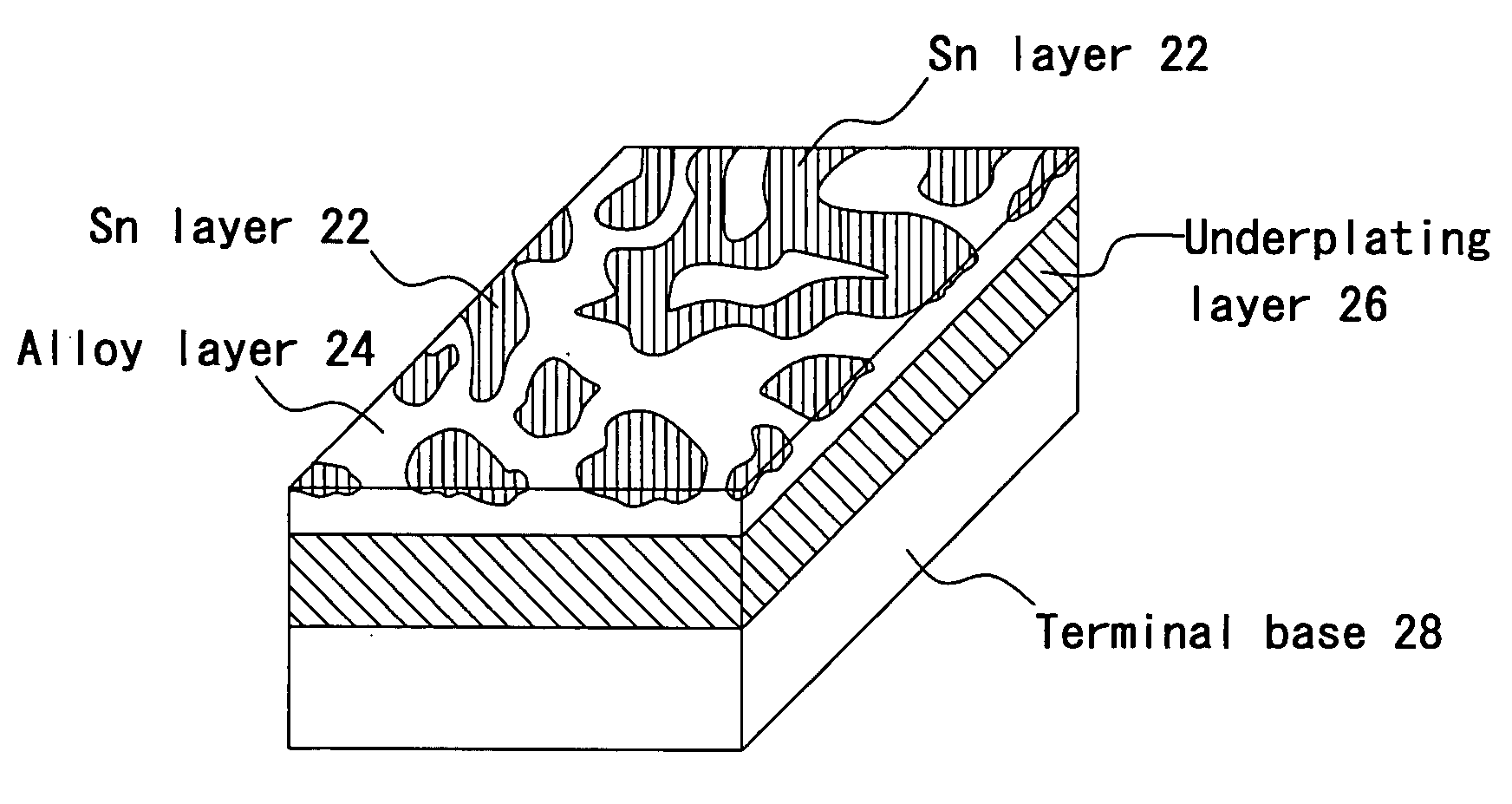
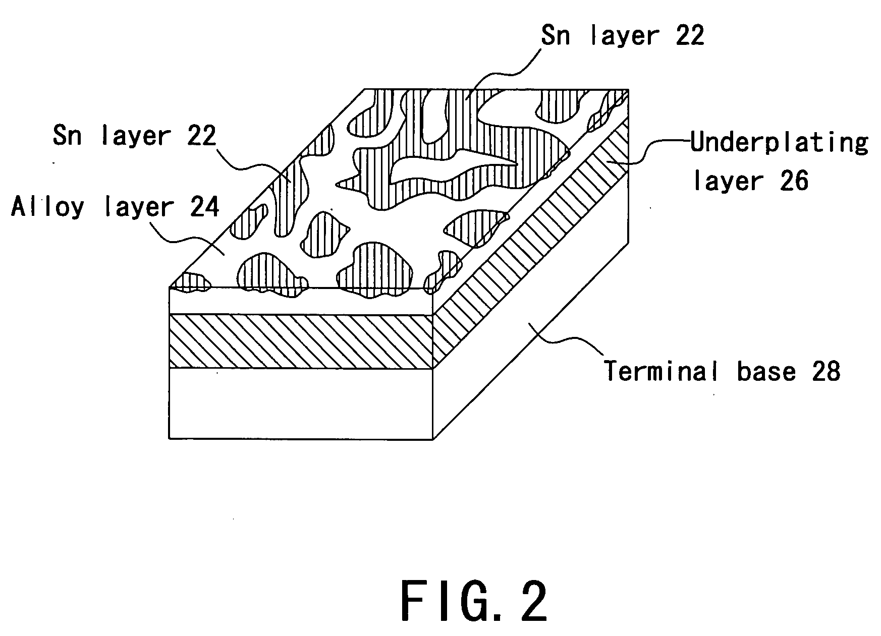
[0080]Ni plating as an underplating layer was provided to a connecting part of a press-fit terminal having a copper based alloy as a base material, and Sn plating at a thickness of 0.4 μm was provided thereto. Then, heating-cooling treatment (of about 30 seconds) was made so that an ultimate maximum temperature became 232-odd ° C. under the temperature conditions shown in FIG. 10, and an Sn—Ni alloy layer was formed on the Ni plating layer.

[0081]Then, a plating surface of the press-fit terminal after the heating-cooling treatment (the reflow process) was observed by an SEM. An SEM image thereof is shown in FIG. 4.

[0082]It was observed from the SEM image in FIG. 4 that white portions 42 and a black portion 44 are mixed. The percentages of Sn and Ni in the while portions 42 and the black portion 44 were measured by AES (Auger Electron Spectroscopy). Results thereof are shown in FIGS. 5A and 5B.

[0083]FIG. 5A shows measurement results on the white portions 42 shown in FIG. 4, and FIG. 5...

examples 2 and 3

[0093]Similar to Example 1, underplating of an Ni metal was provided to connecting parts of press-fit terminals having a copper based alloy as a base material, and Sn plating at a thickness of 0.2 μm and Sn plating at a thickness of 0.7 μm were provided thereto, respectively. Then, heating-cooling treatment (of about 30 seconds) was made so that an ultimate maximum temperature became 232-odd ° C., and Sn—Ni alloy layers were formed on the Ni plating layers. Plating surfaces of the terminals were observed by an SEM, and it was observed, similar to Example 1, that unalloyed Sn was mixed in the outside layers of the Sn—Ni alloy layers.

example 4

[0100]Ni plating and Cu plating as an underplating layer were provided in this order to a connecting part of a press-fit terminal having a copper based alloy as a base material, and Sn plating at a thickness of 0.4 μm was provided thereto. Then, heating-cooling treatment (of about 30 seconds) was made so that an ultimate maximum temperature became 232-odd ° C., and an Sn—Cu alloy layer was formed on the Cu plating layer. The press-fit terminal was press-fitted into and connected to the Cu-plated through hole of the circuit board, and their connection interface was observed by an SIM (Scanning Ion Microscope). In order to test the connection properties in hot environment, the press-fit terminal and the circuit board under connection were let stand for 1000 hours under temperature conditions of 125° C., and a time course change of contact resistance was measured.


PUM

PropertyMeasurementUnit
Temperatureaaaaaaaaaa
Lengthaaaaaaaaaa
Depthaaaaaaaaaa

Abstract

To provide a press-fit terminal with excellent connection reliability of which a plating surface is not scraped off when press-fitted into a through hole of a circuit board.Manufacture of the press-fit terminal for inserting into the conductive through hole of the circuit board includes the steps of forming an underplating layer including one or more plating layers on a surface of a terminal base of a connecting part of the press-fit terminal which comes into electrical contact with the through hole, forming an Sn plating layer on the top plating layer, and after the step of forming the Sn plating layer, conducting a reflow process of performing heat treatment to form an alloy layer of Sn and an underplating metal of the top plating layer on the underplating layer as well as make unalloyed Sn mixed in an outside layer of the alloy layer.

Description

TECHNICAL FIELD[0001]The present invention relates to a press-fit terminal to be inserted into and fit to a through hole of a printed circuit board and the like, specifically, a press-fit terminal of which an Sn plating layer on an outer surface of a connecting part is not scraped off when press-fitted into a through hole of a printed circuit board and the like, a method for manufacturing the press-fit terminal, and a structure of connection between the press-fit terminal and the circuit board.BACKGROUND ART[0002]Conventionally, in electrical connection between a circuit board such as a printed circuit board and connector terminals, it is widely known that the connector terminals are press-fitted into conductive through holes of the circuit board to be mechanically fixed without soldering. The terminal used there is called a press-fit terminal, which has a terminal-inserting part which is inserted into the circuit board, a terminal-attaching part which is inserted into and fit to a ...

Claims


Application Information

Patent Timeline
IPC IPC(8): H01R13/03H01R43/16H01R12/55H01R12/58
CPCH01R12/585Y10T29/49224H01R13/03
Inventor SAITOH, YASUSHI
Owner AUTONETWORKS TECH LTD
Features
  • Generate Ideas
  • Intellectual Property
  • Life Sciences
  • Materials
  • Tech Scout
  • Unparalleled Data Quality
  • Higher Quality Content
  • 60% Fewer Hallucinations
Learn More