Method for manufacturing a phase change memory device with pillar bottom electrode

Active Publication Date: 2008-08-14
GLOBALFOUNDRIES US INC +2
View PDF101 Cites 191 Cited by
  • Summary
  • Abstract
  • Description
  • Claims
  • Application Information

AI Technical Summary

Benefits of technology

[0017]In another variation of the process, a recess is etched in the tops of the electrode pillars prior to deposition of the programmable resistive material. The programmable resistive material fills the recess, creating a region within the programmable resistive material on top of the pillar electrode tending to have higher current density, thereby improving operational characteristic

Problems solved by technology

Although this technique is suitable for forming very small bottom electrode structures using plugs in vias, it has proved to suffer reliability and yield issues.
For example, as described by Ahn et al., it has proven difficult to form reliable contact with the underlying access circuitry at the bottom of very small vias.
This results in some cells in the array permanently disconnected from the access circuits.
Furthermore, Ahn et al. have related that it is difficult to ensure in the plug-in-via process that the areas of the exposed tops of the plug electrodes are uniform after the planarizing step across a large array of such cells.
This problem is exacerbated by the techniques used in attempts to successfully fill the vias, including depositing thin films and anisotropic etching of the thin films to

Method used


Image

  • Method for manufacturing a phase change memory device with pillar bottom electrode
  • Method for manufacturing a phase change memory device with pillar bottom electrode
  • Method for manufacturing a phase change memory device with pillar bottom electrode

Examples


Example

[0029]The following detailed description is made with reference to the figures. Those of ordinary skill in the art will recognize a variety of equivalent variations on the description that follows.

[0030]With regard to directional descriptions herein, the orientation of the drawings establish their respective frames of reference, with “up,”“down,”“left” and “right” referring to directions shown on the respective drawings. Similarly, “thickness” refers to a vertical dimension and “width” to the horizontal. These directions have no application to orientation of the circuits in operation or otherwise, as will be understood by those in the art.

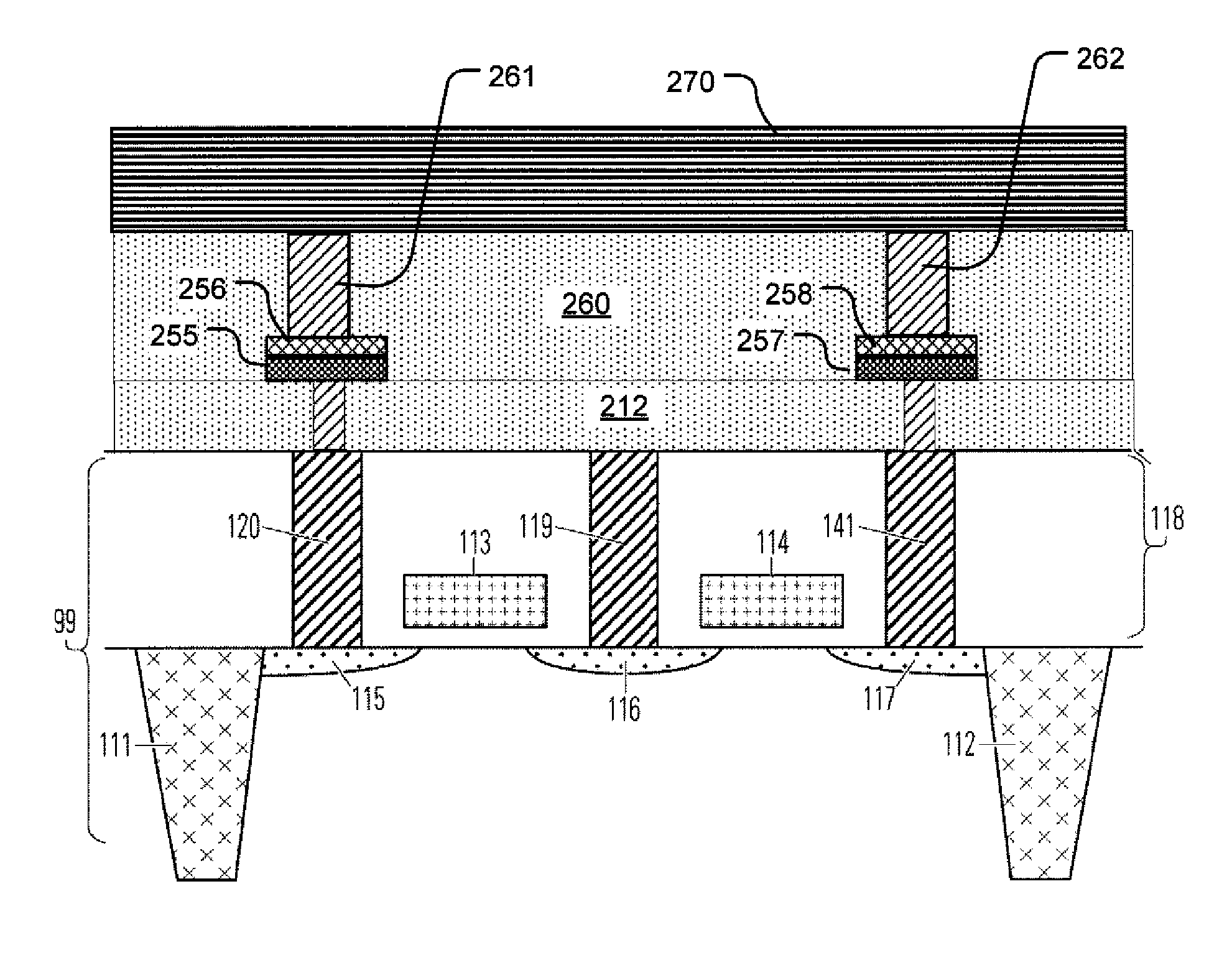
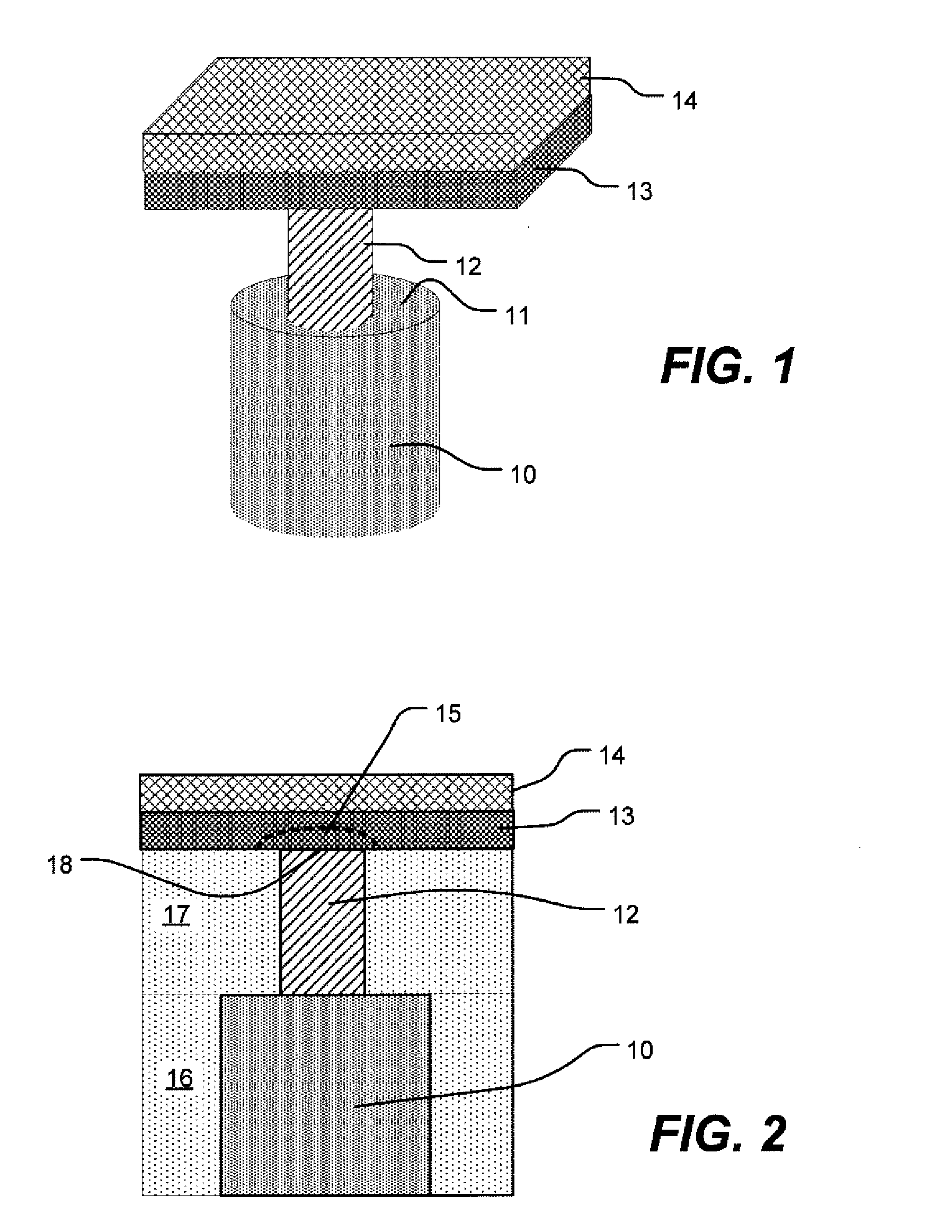
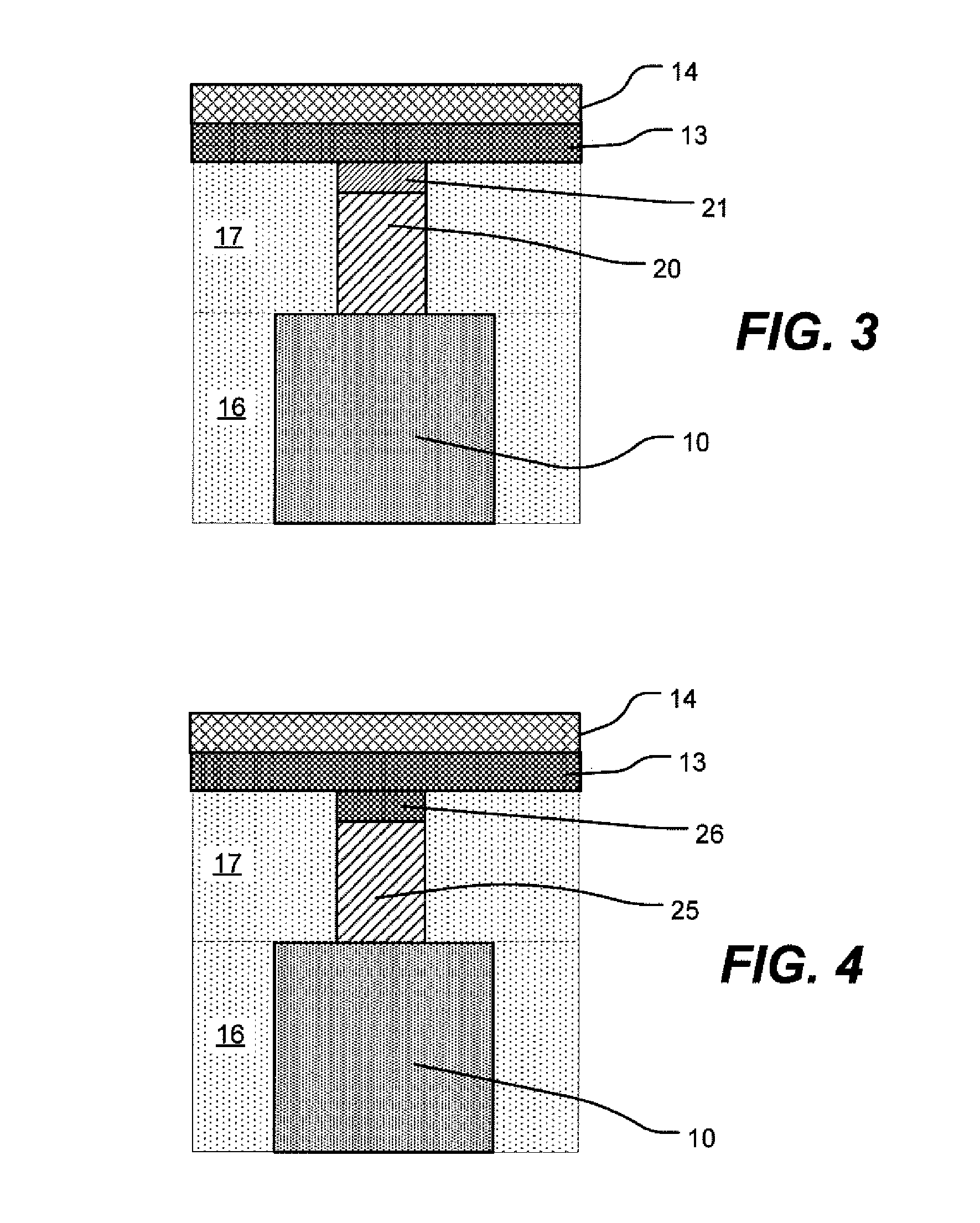
[0031]FIG. 1 provides a prospective view of the basic structure of a phase change memory cell manufactured as described herein with dielectric fill material removed from the drawing. The memory cell is formed on a contact 10 having a contact surface 11. Contact 10 comprises a “plug” extending through an inter-layer dielectric to underlying access c...


PUM


Abstract

A method for manufacturing a mushroom-cell type phase change memory is based upon manufacturing a pillar of bottom electrode material upon a substrate including an array of conductive contacts in electrical communication with access circuitry. A layer of electrode material is deposited making reliable electrical contact with the array of conductive contacts. Electrode material is etched to form a pattern of electrode pillars on corresponding conductive contacts. Next, a dielectric material is deposited over the pattern and planarized to provide an electrode surface exposing top surfaces of the electrode pillars. Next, a layer of programmable resistive material, such as a chalcogenide or other phase change material, is deposited, followed by deposition of a layer of a top electrode material. A device including bottom electrode pillars with larger bottom surfaces than top surfaces is described.

Description

REFERENCE TO RELATED APPLICATION[0001]This application claims the benefit of U.S. Provisional Patent Application No. 60 / 889,415, filed 12 Feb. 2007 by the same co-inventors, entitled Method for Manufacturing a Phase Change Memory Device with Pillar Bottom Electrode, which is incorporated by reference herein.BACKGROUND OF THE INVENTION[0002]1. Field of the Invention[0003]The present invention relates to methods for manufacturing high density memory devices based on phase change based memory materials, including chalcogenide based materials and other materials, and most particularly to methods for manufacturing a phase change memory element with a pillar-shaped bottom electrode.[0004]2. Description of Related Art[0005]Phase change based memory materials are widely used in nonvolatile random access memory cells. Such materials, such as chalcogenides and similar materials, can be caused to change phase between an amorphous state and a crystalline state by application of electrical curre...

Claims


Application Information

Patent Timeline
IPC IPC(8): H01L45/00
CPCG11C13/0004H01L27/2436H01L45/04H01L45/06H01L45/1233H01L45/126H01L45/1675H01L45/144H01L45/146H01L45/147H01L45/148H01L45/1625H01L45/1641H01L45/14
Inventor LUNG, HSIANG LANCHEN, CHIEH-FANGCHEN, YI-CHOUCHEN, SHIH HUNGLAM, CHUNG HONJOSEPH, ERIC ANDREWSCHROTT, ALEJANDRO GABRIELBREITWISCH, MATTHEW J.BURR, GEOFFREY WILLIAMHAPP, THOMAS D.PHILIPP, JAN BORIS
Owner GLOBALFOUNDRIES US INC
Why Eureka
Try Eureka