Organic light emitting diode device and method of manufacturing the same

a light-emitting diode and organic technology, which is applied in the direction of organic semiconductor devices, discharge tube luminescnet screens, other domestic articles, etc., can solve the problems of difficult to form both and the injection layer and the injection layer cannot be formed in the organic light-emitting diode device. , to achieve the effect of increasing light-emitting efficiency and lifespan

Active Publication Date: 2008-08-14
LG DISPLAY CO LTD
View PDF2 Cites 23 Cited by
  • Summary
  • Abstract
  • Description
  • Claims
  • Application Information

AI Technical Summary

Benefits of technology

[0015]An advantage of the present invention is to provide an organic light emitting diode device that has an increased light emitting efficiency and lifespan.
[0016]Another advantage of the present invention is to provide an organic light emitting diode device that can be manufactured using a large substrate through a simple wet process.
[0017]Additional features and advantages of the invention will be set forth in the description which follows, and in part will be apparent from the description, or may be learned from practice of the invention. These and other advantages of the invention will be realized and attained by the structure and method particularly pointed out in the written description and claims hereof as well as the appended drawings.
[0018]To achieve these and other advantages and in accordance with the purpose of the invention, as embodied and broadly described herein, an organic light emitting diode device includes: a first electrode formed on a substrate; at least one organic layer formed on the first electrode; an organic light emitting layer formed on the organic layer; and a second electrode formed on the organic light emitting layer, wherein the organic layer is formed of a compound represented by Formula 1 below:
[0019]In another aspect of the present invention, a method of manufacturing an organic light emitting diode device includes: forming a first electrode on a substrate; forming at least one organic layer on the first electrode; forming an organic light emitting layer on the organic layer; and forming a second electrode on the organic light emitting layer, wherein the organic layer is formed of a compound represented by Formula 1 below:
[0020]It is to be understood that both the foregoing general description and the following detailed description are exemplary and explanatory and are intended to provide further explanation of the invention as claimed.

Problems solved by technology

Furthermore, when a hole injection layer is formed under the hole transport layer, it is more difficult to select solvents for the respective layers.
For this reason, when an organic light emitting diode device is manufactured using a wet process, it is difficult to form both the hole injection layer and the hole transport layer.
Therefore, although the organic light emitting layer is formed in the organic light emitting diode device, both the hole injection layer and the hole transport layer cannot be formed in the organic light emitting diode device (that is, only one of the hole injection layer and the hole transport layer is formed).
Moreover, it is also difficult to select materials for the hole injection layer and the hole transport layer.

Method used


Image

  • Organic light emitting diode device and method of manufacturing the same
  • Organic light emitting diode device and method of manufacturing the same
  • Organic light emitting diode device and method of manufacturing the same

Examples


first embodiment

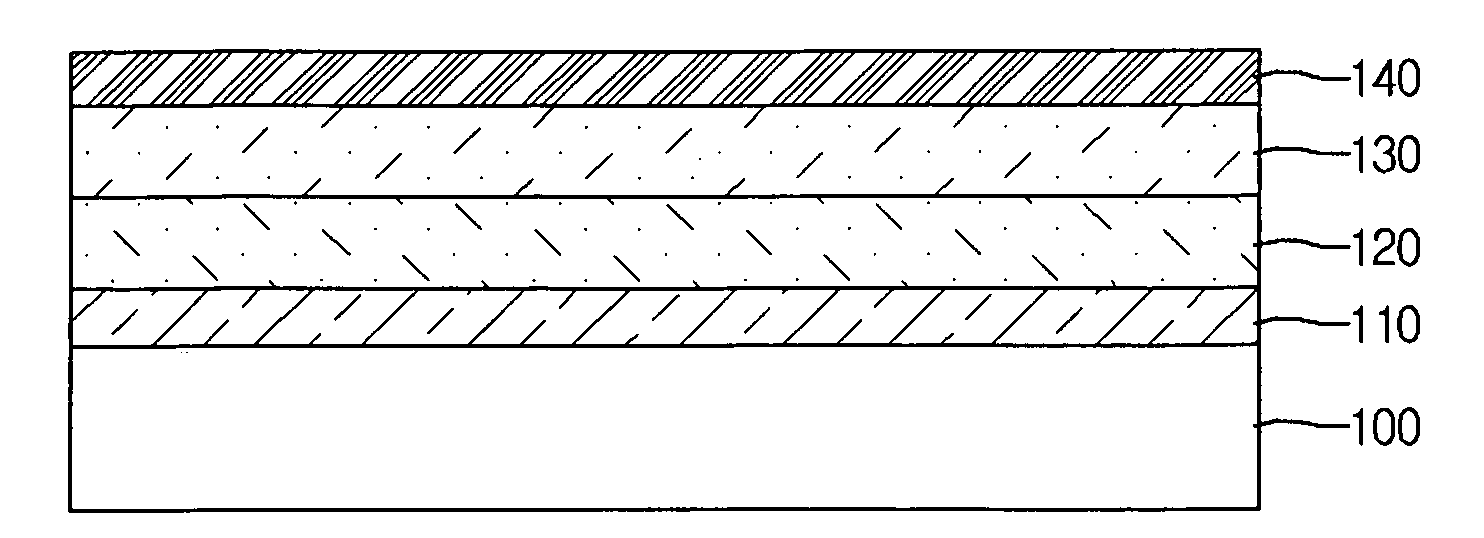
[0027]FIG. 1 is sectional view illustrating an organic light emitting diode device according to a first embodiment of the present invention. In the following description of the current embodiment, only one organic light emitting diode device included in a pixel will be described for clarity although a number of pixels are used for displaying an image.

[0028]Referring to FIG. 1, the organic light emitting diode device includes a first electrode 110, an organic layer 120, an organic light emitting layer 130, and a second electrode 140 that are sequentially formed on a substrate 100.

[0029]For example, a plastic substrate, a glass substrate, or a film substrate can be used as the substrate 100. Particularly, when light is transmitted through the substrate 100, the substrate 100 may be formed of a transparent substrate.

[0030]The first electrode 110 is formed on the substrate 100. The first electrode 110 may be an anode that supplies holes to the organic light emitting layer 130. The first...

second embodiment

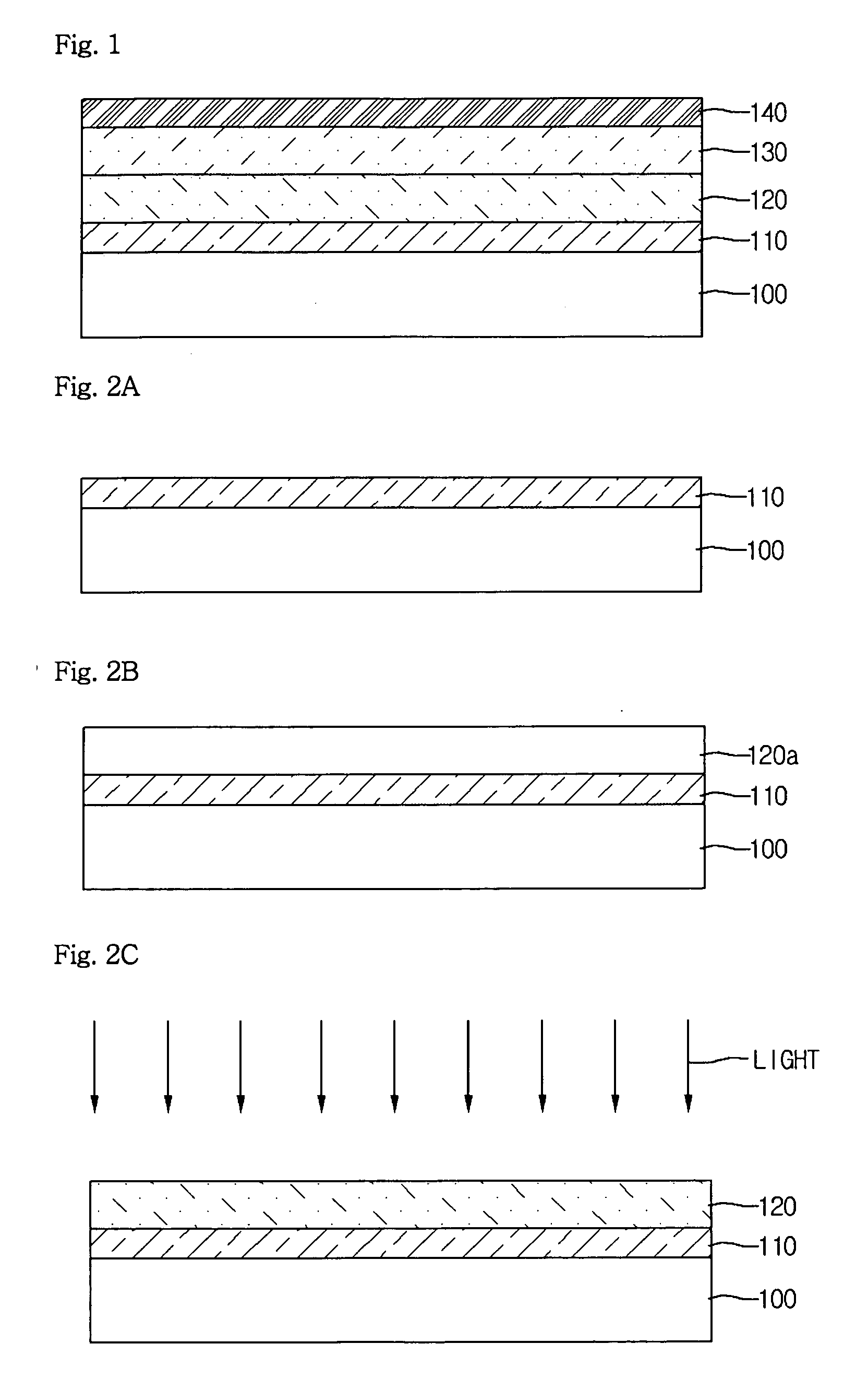
[0048]FIGS. 2A, 2B, 2C and 2D are sectional views for explaining a method of manufacturing an organic light emitting diode device according to a second embodiment of the present invention.

[0049]Referring to FIG. 2A, to form an organic light emitting diode device, a first electrode 110 is formed on a substrate 100. The first electrode 110 may be formed of a transparent conductive material. For example, the first electrode 110 may be formed of ITO or IZO. The first electrode 110 can be formed by sputtering.

[0050]Referring to FIG. 2B, a preliminary organic layer 120a is formed on the first electrode 110. The preliminary organic layer 120a may be formed of a composition including a compound represented by formula 1 below and a photo initiator.

R1−(R2)n   [Formula 1]

where R1 may be at least one selected from the group consisting of a diamine derivative, an arylene diamine derivative, a carbazole derivative, a spiro-arylene diamine derivative, and a starburst amine derivative. For example,...

third embodiment

st Organic Layer

[0068]A substrate 100 is prepared to form a first organic layer on the substrate 100. A cleaned glass substrate is used as the substrate 100.

[0069]The first organic layer is formed on the substrate 100 to a thickness of 600 A. The first organic layer is formed of a compound represented by Formula 1. That is, the first organic layer is formed of N,N′-Bis-(3-methylphenyl)-N,N′-bis-(phenyl)-benzidine(TPD) having an oxetane group. The first organic layer is formed through a spin coating process (wet process).


PUM


Abstract

An organic light emitting diode device includes an organic layer formed of a hole transport material or a hole injection material having a photocurable group. Therefore, the organic light emitting diode device can be formed using a wet process that is simple and can be used for a large substrate. Furthermore, the organic layer and an organic light emitting layer are less affected by a solvent,. Thus, the lifespan of the organic light emitting diode device is increased and there is more freedom in selecting materials for the organic layer and the organic light emitting layer. A method of manufacturing the organic light emitting diode device is also disclosed.

Description

[0001]This application claims the benefit of Korean Patent Application No. 10-2007-0013768, filed on Feb. 9, 2007, which is hereby incorporated by reference for all purposes as if fully set forth herein.BACKGROUND OF THE INVENTION[0002]1. Field of the Invention[0003]The present invention relates to an organic light emitting diode device and a method of manufacturing the organic light emitting diode device, and more particularly, to an organic light emitting diode device that can be manufactured using a wet process and a method of manufacturing the organic light emitting diode device.[0004]2. Description of the Related Art[0005]An organic light emitting diode device includes an anode, a cathode, and an organic light emitting layer disposed between the anode and the cathode. In the organic light emitting diode device, electrons and holes are supplied from the cathode and the anode to the organic light emitting layer and are recombined with each other. Then, light is emitted from the o...

Claims


Application Information

Patent Timeline
Patent Type & Authority Applications(United States)
IPC IPC(8): B05D5/12H01J1/63
CPCH01L51/005H01L51/0059H01L2251/308H01L51/5048H01L51/5088H01L51/0072Y10S428/917H10K85/60H10K85/631H10K85/6572H10K50/14H10K50/17H10K2102/103C09K11/06
Inventor CHAE, GEE SUNGKIM, SUNG HEEPARK, TAE HAN
Owner LG DISPLAY CO LTD
Why Eureka
Try Eureka